WIRELESS COMMUNICATIONS DIVISION
For additional information and latest specifications, see our website: www.triquint.com
1
Product Description
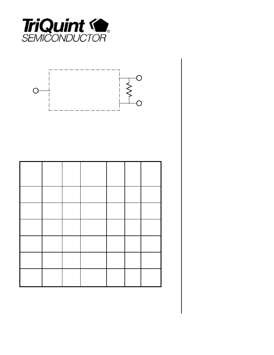
The TQ1303 through TQ1308 are a family of passive power splitters. These devices are used
to split one input power into two output powers, with minimal degradation. The input and
outputs are matched to 50 ohms and by keeping the100 ohm resistor off-chip it allows for high
power capacity.
P/N
Freq.
(MHz)
Amp
Bal.
(dB)
Phase
Deviation
(degrees)
I.L.
(dB)
(max)
Isol.
(dB)
VSWR
(max)
TQ1303
741
+-19
<1
(max)
0
∞
+- 3
o
(max)
3.5
+-0.5
14
(min)
1.7
TQ1304
967
+-13
<1
(max)
0
∞
+-3
o
(max)
3.5
+-0.5
18
(min)
1.6
TQ1305
1370
+-30
<1
(max)
0
∞
+-3
o
(max)
3.5
+-0.5
20
(min)
1.5
TQ1305
1406
+-6
<1
(max)
0
∞
+-3
o
(max)
3.5
+-0.5
19.5
(min)
1.5
TQ1305
1412
+-47.5
<1
(max)
0
∞
+-3
o
(max)
3.5
+-0.5
18
(min)
1.5
TQ1308
2140
+-20
<1
(max)
0
∞
+-3
o
(max)
3.4
+-0.5
17
(min)
1.7
Note: Min/Max limits are -40 to +85
∞
C case temperatures, unless otherwise specified.
TQ1303-TQ1308
DATA SHEET
0
∞
∞
∞
∞
Power Splitters
Features
Small size: MLF 2x2
Less than <3
∞
Phase Deviation
Excellent Isolation
Low VSWR
Less than <1 dB Amplitude Balance
Applications
Wireless Communications
Power Sensing/Level Sensing
Reflectometers
Amplifier Combining
General Purpose Apps
IN
OUT 2
OUT 1
Splitter
100
ohm

TQ1303-1308
Data Sheet
For additional information and latest specifications, see our website: www.triquint.com
2
Absolute Maximum Ratings
Parameter
Value
Units
Operating Temperature
-40 to 85
∞
C
Storage Temperature
-60 to 150
∞
C
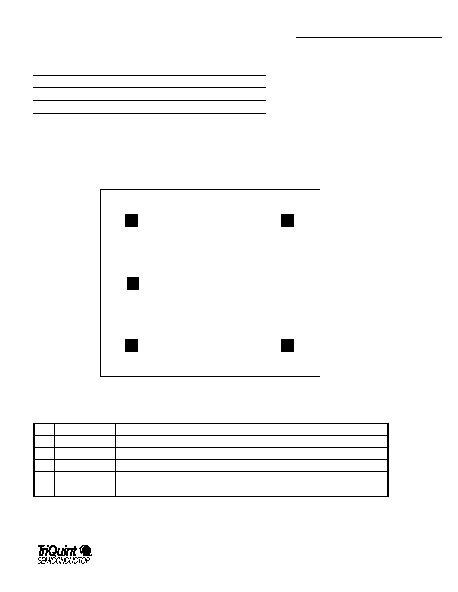
Block Diagram: TQ1303-TQ1308
Pin 4
OUT 2
Pin 5
GND
Pin 3
OUT 1
Pin 1
INPUT
Pin 2
GND
PIN-OUT FUNCTIONAL DESCRIPTION
Pin
Name
Description
1
INPUT
RF Input
2
GND
Ground
3
OUT 1
Output 1 port
4
OUT 2
Output 2 port
5
GND
Ground

TQ1303-1308
Data Sheet
For additional information and latest specifications, see our website: www.triquint.com
3
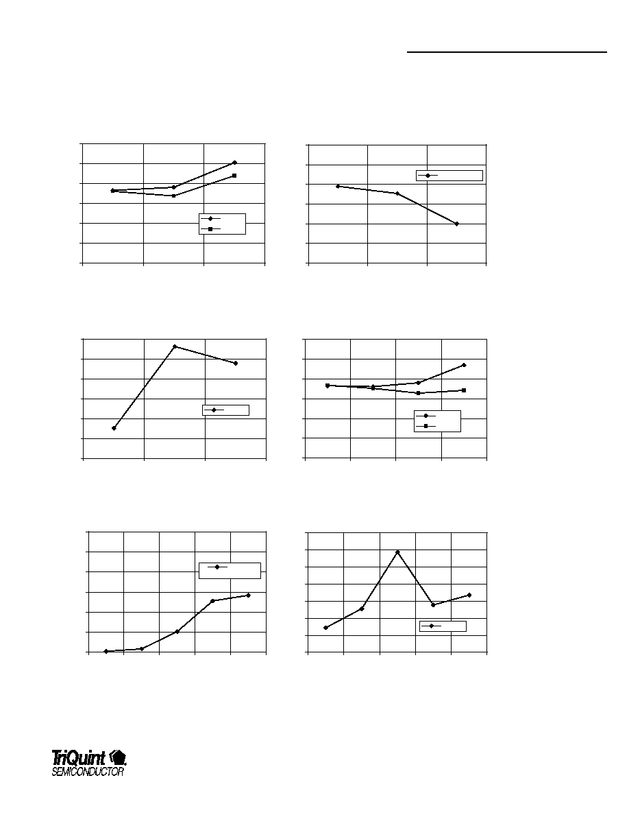
Typical Performance
Test Conditions, unless Otherwise Specified: Tc=+25C
TQ1303 Amplitude Balance
0
0.5
1
1.5
2
2.5
3
500
1000
1500
2000
2500
Frequency (MHz)
Ampl
i
t
ude Bal
a
nce (
d
B)
Amplitude
Balance
TQ1303 Isolation
0
5
10
15
20
25
500
750
1000
1250
Frequency (MHz)
I
s
ol
at
i
on (
d
B)
Isolation
TQ1303 Phase Deviation
-3
-2
-1
0
1
2
3
500
1000
1500
Frequency (MHz)
Phase Devi
at
i
on (
d
egr
ees)
Phase Deviation
TQ1304 Amplitude Balance
0
0.5
1
1.5
2
2.5
3
500
1000
1500
2000
2500
Frequency (MHz)
Ampl
i
t
ude Bal
a
nce (
d
B)
Amplitude Balance
TQ1303 Insertion Loss
0
1
2
3
4
5
6
7
500
1000
1500
Frequency (MHz)
I
n
ser
t
i
on Loss (
d
B)
Output 1
Output 2
TQ1304 Phase Deviation
-3
-2
-1
0
1
2
3
500
1000
1500
Frequency (MHz)
Phase Devi
at
i
on (
d
egr
ees)
Phase Deviation

TQ1303-1308
Data Sheet
For additional information and latest specifications, see our website: www.triquint.com
6
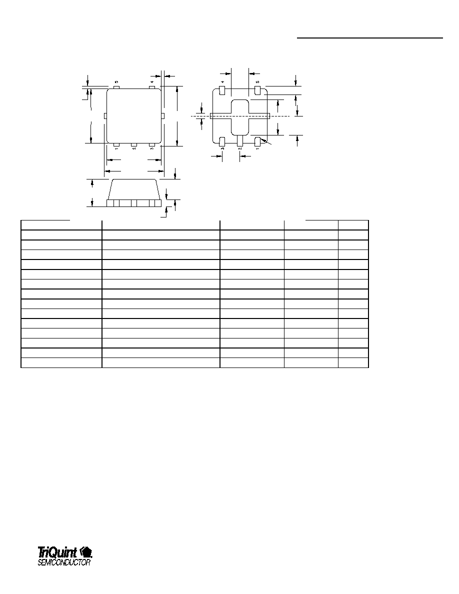
Package Dimensions:
JEDEC DESIGNATION
DESCRIPTION
METRIC
ENGLISH
NOTE
A
OVERALL HEIGHT
0.90 +/-.10 mm
.035 +/-.004 in
1
A2
PACKAGE BODY HEIGHT
0.70 +/-.05mm
.028 +/-.002 in
1
A3
PACKAGE BASE HEIGHT
0.20 +/-.05mm
.008 +/-.002 in
1
r
LEAD RADIUS
0.075 mm REF
.003 in
1
b
TERMINAL WIDTH
0.23 +/-.05 mm
.009 +/-.002 in
1
D
PACKAGE LENGTH
2.00 mm BSC
.079 in
1
D2
EXOPSED PAD LENGTH
1.324 +/-0.1 mm
.052 +/-.004 in
1
e
TERMINAL PITCH
0.65 mm BSC
.026 in
1
E
PACKAGE WIDTH
2.00 mm BSC
.079 in
1
E2
EXPOSED PAD WIDTH
0.624 +/-0.1 mm
.025 +/-.004 in
1
E4
PAD END TO CENTERLINE
0.662 +/-0.1 mm
.026 +/-.004 in
1
L
TERMINAL LENGTH
0.355 +/-.14 mm
.014 +/-.006 in
1
L2
TERMINAL PAST BODY LENGTH
0.063 mm REF
.03 in
1
L3
TERMINAL PAST BODY WIDTH
0.063 mm REF
.03 in
1
1.
Notes: PRIMARY DIMENSIONS ARE IN METRIC MILLIMETERS. THE ENGLISH EQUIVALENTS ARE CALCULATED AND SUBJECT TO
ROUNDING ERROR.
Additional Information
For latest specifications, additional product information, worldwide sales and distribution locations, and information about TriQuint:
Web: www.triquint.com
Tel: (503) 615-9000
Email: info_wireless@tqs.com
Fax: (503) 615-8900
For technical questions and additional information on specific applications:
Email: info_wireless@tqs.com
The information provided herein is believed to be reliable; TriQuint assumes no liability for inaccuracies or omissions. TriQuint assumes no responsibility for the use of this
information, and all such information shall be entirely at the user's own risk. Prices and specifications are subject to change without notice. No patent rights or licenses to any of
the circuits described herein are implied or granted to any third party.
TriQuint does not authorize or warrant any TriQuint product for use in life-support devices and/or systems.
Copyright © 1998 TriQuint Semiconductor, Inc. All rights reserved.Revision A, October, 2001
A
A2
A3
L2
L3
E2
L
b1
e
D2
r
E4
E
E1
D1
D
