 | –≠–ª–µ–∫—Ç—Ä–æ–Ω–Ω—ã–π –∫–æ–º–ø–æ–Ω–µ–Ω—Ç: TQ2060 | –°–∫–∞—á–∞—Ç—å:  PDF PDF  ZIP ZIP |
T
R
I Q
U
I
N
T
S E M I C O N D U C T O R , I N C .
1
SYSTEM TIMING
PRODUCTS
For additional information and latest specifications, see our website: www.triquint.com
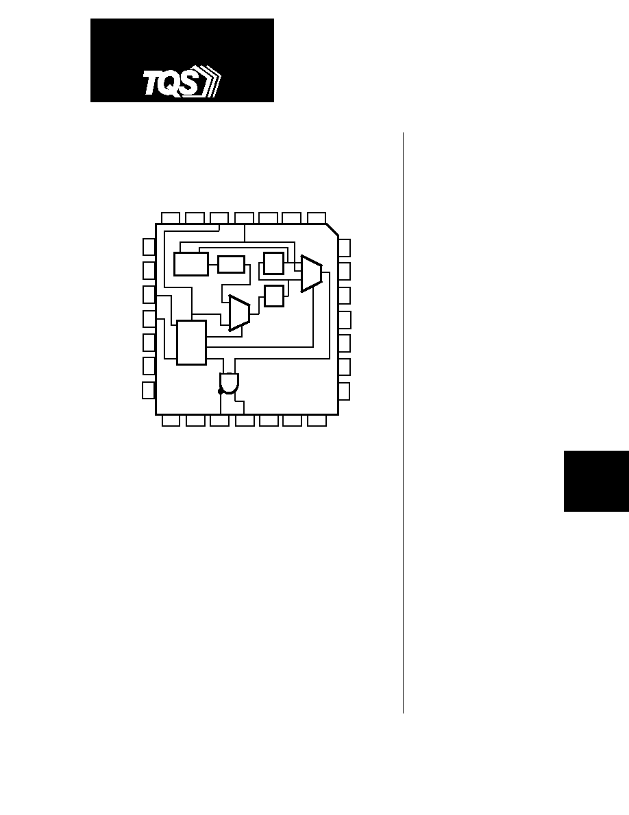
Figure 1. Pinout Diagram
TQ2060
High-Frequency
Clock Generator
Features
∑ Output frequency range:
350 MHz to 500 MHz
∑ One differential PECL output:
600 mV (min) swing
∑ Common-mode voltage:
V
DD
≠1.2 V (max),
V
DD
≠1.6 V (min)
∑ Period-to-period output jitter:
25 ps peak-to-peak (typ)
70 ps peak-to-peak (max)
∑ Reference clock input:
35 MHz to 50 MHz TTL-level
crystal oscillator
∑ Self-contained loop filter
∑ Optional 200-ohm pull-down
resistors for AC-coupled outputs
∑ +5 V power supply
∑ 28-pin J-lead surface-mount
package
∑ Ideal for designs based on
DEC Alpha AXP
TM
processors
TriQuint's TQ2060 is a high-frequency clock generator. It utilizes a 35 MHz
to 50 MHz TTL input to generate a 350 MHz to 500 MHz PECL output. The
TQ2060 has a completely self-contained Phase-Locked Loop (PLL) running
at 700 MHz to 1000 MHz. This stable PLL allows for a low period-to-period
output jitter of 70 ps (max), and enables tight duty cycle control of
55% to 45% (worst case).
The TQ2060 provides optional 200 ohm on-chip pull-down resistors which
are useful if the output is AC-coupled to the device being driven. In order
to use these resistors, pin 20 (PDR2) should be connected to pin 21 (QN),
and pin 23 (PDR1) should be connected to pin 22 (Q).
Various test modes on the chip simplify debug and testing of systems by
slowing the clock output or by bypassing the PLL.
AVDD
1
4
3
2
NC
NC
NC
NC
NC
NC
AGND
GND
PDR1
Q
QN
PDR2
EVDD
VDD
NC
GND
NC
NC
TEST1
28
27
26
19
20
21
22
23
24
25
11
10
9
8
7
6
5
16
17
18
13
12
15
14
NC
NC
GND
REFCLK
TESTIN
NC
GND
Control
Phase
Detector
VCO
MUX
˜
2
MUX
˜
10
TEST2
TQ2060
2
For additional information and latest specifications, see our website: www.triquint.com
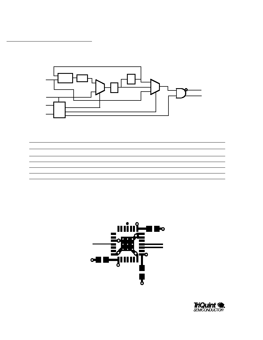
Mode
TEST1
TEST2
TESTIN
1
REFCLK
Q, QN
1(Test)
0
0
f
TESTCLK
"don't care"
f
REFCLK
2
˜
20
2 (Test)
0
1
"don't care"
"don't care"
0, 1
3 (Test)
1
0
f
TESTCLK
"don't care"
f
TESTCLK
˜
2
4 (Bypass)
1
1
0
f
REFCLK
f
REFCLK
5 (Normal
1
1
1
f
REFCLK
10 x f
REFCLK
3
Figure 2. Simplified Block Diagram
Table 1. Mode Selection
Notes: 1. In modes 1 and 3, TESTIN may be used to bypass the PLL. A clock input at TESTIN will be divided as shown.
2. REFCLK = 35 MHz to 50 MHz.
3. Q, QN = 350 MHz to 500 MHz.
Pin 1
Q
QN
REFCLK
(from TTLoscillator)
GND
VDD
VDD
VDD
GND
GND
GND
0.1
µ
F
0.1
µ
F
0.1
µ
F
50 OHMS
Figure 3. Recommended Layout
(Not to scale)
(From TTL Oscillator)
(35MHz to
50 MHz)
Phase
Detector
˜
2
REFCLK
TESTIN
TEST1
TEST2
Q
QN
MUX
MUX
VCO
Control
˜
10
(350 MHz
to
500 MHz)
TQ2060
3
SYSTEM TIMING
PRODUCTS
For additional information and latest specifications, see our website: www.triquint.com
Table 2. Absolute Maximum Ratings
Storage Temperature
≠65
∞
C to +150
∞
C
Ambient temperature with power applied
≠55
∞
C to +110
∞
C
Supply voltage to ground potential
≠0.5 V to +7.0 V
DC input voltage
≠0.5 V to (V
DD
+ 0.5) V
DC input current
≠30 mA to +5 mA
Package thermal resistance (MQuad)
JA
= 45
∞
C/W
Die junction temperature
T
J
= 150
∞
C
Note:
Stresses above those listed in Absolute Maximum Ratings may cause permanent damage to the device.
The device should be operated only under the DC and AC conditions shown below.
Table 3. DC Characteristics (V
DD
= +5 V + 5%, T
A
= 0
∞
C to +70
∞
C)
1
Symbol
Description
Test Conditions
Min
Typ
Max
Unit
V
OH
Output HIGH voltage
V
CC
= Min PECL load
V
CC
≠1.20
V
CC
≠0.50
V
V
OL
Output LOW voltage
V
CC
= Min PECL load
V
CC
≠2.00
V
CC
≠1.60
V
V
CMO
Output common mode voltage
PECL
V
CC
≠1.60
V
CC
≠1.20
V
V
OUT
Output differential voltage
PECL
0.6
1.2
V
V
IH
2
Input HIGH level
Guaranteed input logical
2.0
V
HIGH Voltage for all inputs
V
IL
2
Input LOW level
Guaranteed input logical
0.8
V
LOW Voltage for all inputs
I
IL
Input LOW current
V
DD
= Max V
IN
= 0.40 V
≠150
≠400
µ
A
I
IH
Input HIGH current
V
DD
= Max V
IN
= 2.7 V
0
25
µ
A
I
I
Input HIGH current
V
DD
= Max V
IN
= 5.3 V
2
1000
µ
A
I
DDS
3
Power supply current
V
DD
= Max
85
120
mA
V
I
Input clamp voltage
V
DD
= Min I
IN
= ≠18 mA
≠0.70
≠1.2
V
Table 4. Capacitance
Symbol
Description
Test Conditions
Min
Typ
Max
Unit
C
IN
Input Capacitance
V
IN
= 2.0 V at f = 1 MHz
6
pF
C
OUT
Output Capacitance
V
OUT
= 2.0 V at f = 1 MHz
9
pF
Notes: 1. Typical limits are at V
DD
= 5.0 V and T
A
= 25∞C.
2. These are absolute values with respect to device ground and include all overshoots due to system or tester noise.
3. This parameter is measured with device not switching and unloaded.
TQ2060
4
For additional information and latest specifications, see our website: www.triquint.com
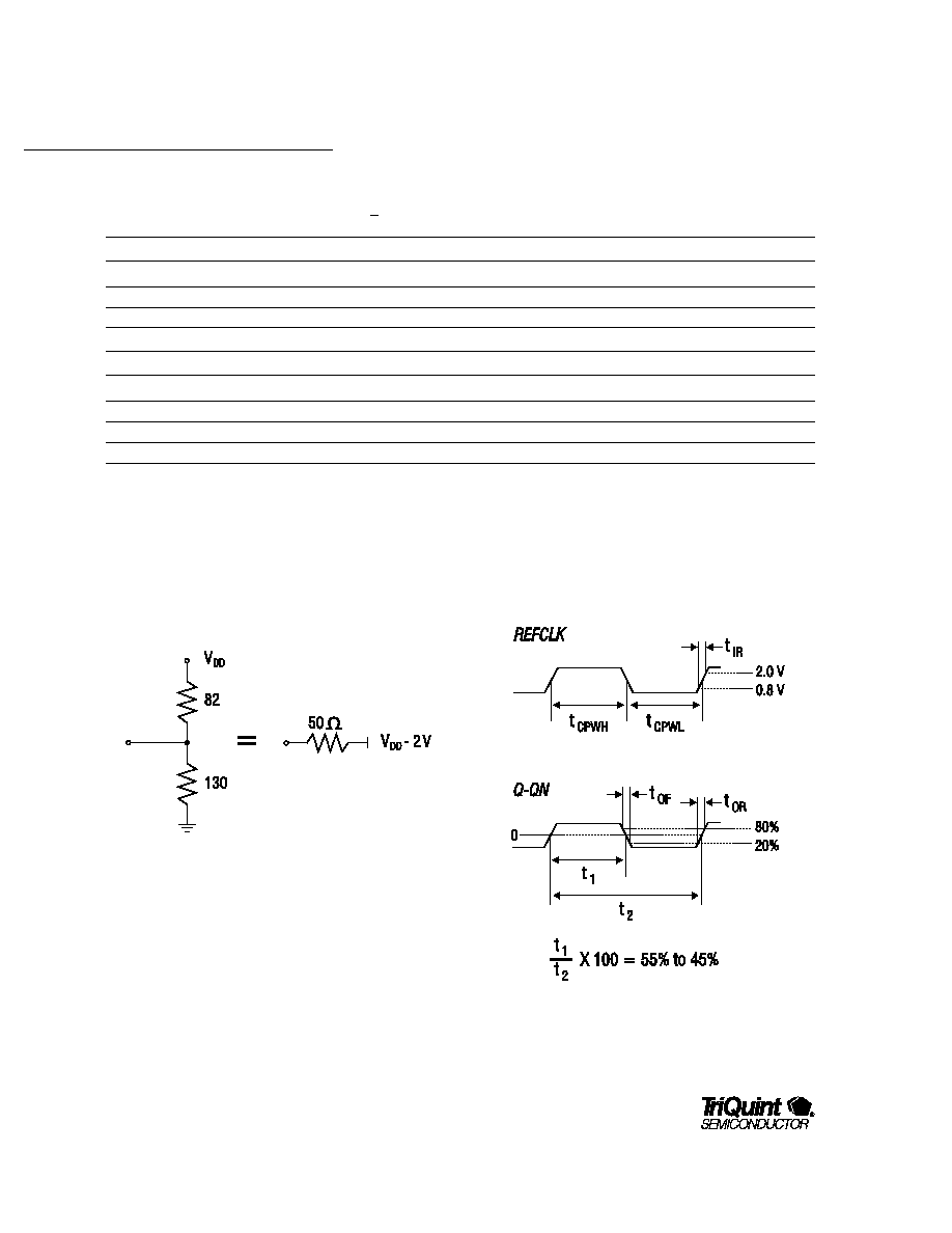
Table 5. AC Characteristics (V
DD
= +5 V
+ 5%, T
A
= 0
∞
C to +70
∞
C)
Symbol
Input Clock (REFCLK)
Test Conditions (Figure 5)
Min
Typ
Max
Unit
t
CPWH
CLK pulse width HIGH
Figure 5
4
--
--
ns
t
CPWL
CLK pulse width LOW
Figure 5
4
--
--
ns
t
IR
Input rise time (0.8 V ≠ 2.0 V)
--
--
2.0
ns
Symbol
Output Clock (Q, QN)
Test Conditions (Figures 4 & 5)
1
Min
Typ
Max
Unit
t
OR,
t
OF
Rise/fall time (20% ≠ 80%)
Figure 5
100
220
350
ps
t
CYC
Duty-cycle
Figure 5
45
50
55
%
t
JP
2
Period-to-Period Jitter
--
25
70
ps
t
SYNC
3
Synchronization Time
--
10
500
µ
s
Notes: 1. All measurements are tested with a REFCLK having a rise time of 0.5 ns (0.8 V to 2.0 V).
2. Jitter specification is peak to peak. Period-to-Period jitter is the jitter on the output with respect to the output's previous crossing.
3. t
SYNC
is the time required for the PLL to synchronize and assumes the presence of a CLK signal.
Figure 5. REFCLK and Q-QN Timing
Figure 4. PECL Test Load
TQ2060
5
SYSTEM TIMING
PRODUCTS
For additional information and latest specifications, see our website: www.triquint.com
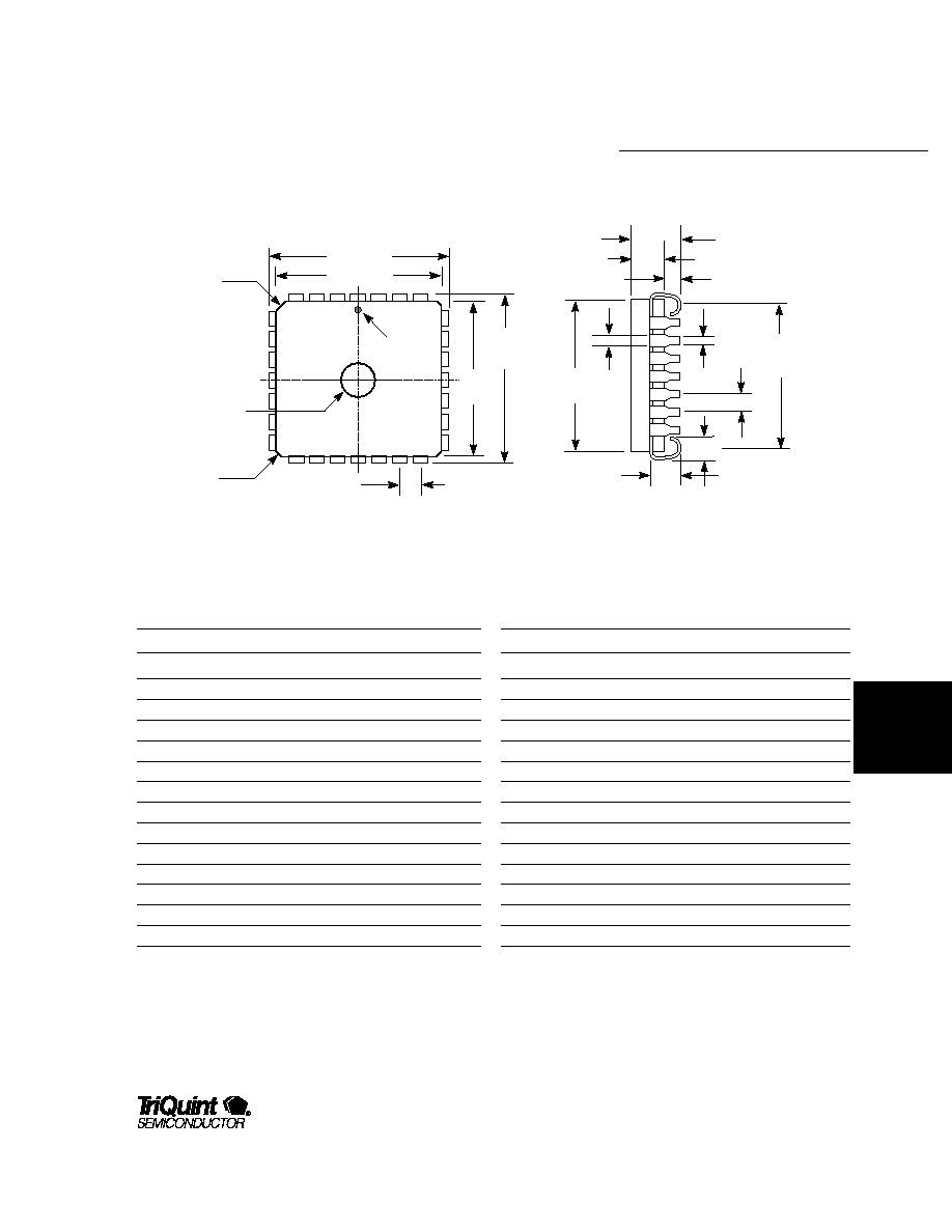
Table 6. 28-Pin MQuad Pin Description
Pin #
Pin Name
Description
I/O
1
NC
No Connect
--
2
NC
No Connect
--
3
NC
No Connect
--
4
NC
No Connect
--
5
NC
No Connect
--
6
NC
No Connect
--
7
GND
Ground
--
8
REFCLK
Reference Clock
I
9
TESTIN
Test Input
I
10
NC
No Connect
--
11
GND
Logic Ground
--
12
VDD
Logic VDD (+5 V)
--
13
NC
No Connect
--
14
TEST1
Test Control 1
I
Figure 6. 28-Pin MQuad J-Leaded Package Mechanical Specification
Pin #
Pin Name
Description
I/O
15
TEST2
Test Control 2
I
16
NC
No Connect
--
17
NC
No Connect
O
18
GND
Ground
--
19
EVDD
VDD for ECL Output (+5 V)
--
20
PDR2
Pull-down Resistor 2 (200
)
I
21
QN
Differential PECL Output (≠)
O
22
Q
Differential PECL Output (+)
O
23
PDR1
Pull-down Resistor 1 (200
)
I
24
GND
Ground
--
25
AGND
Analog Ground
--
26
AVDD
Analog VDD (+5 V)
--
27
NC
No Connect
--
28
NC
No Connect
--
(All dimensions in inches)
PIN 1
.050 TYP.
NON-ACCUM.
.445 ±.005
.490 ±.005
.445
±.005
.490
±.005
.045
X 45∞∞
.132 ±.005
.050 TYP.
.410
±.015
.018
.104
±.005
.172 ±.005
8
15
22
.445
±.005
.040 MIN
.015
X 45∞∞
0.125
VENT PLUG
.028
.060

TQ2060
6
For additional information and latest specifications, see our website: www.triquint.com
Additional Information
For latest specifications, additional product information,
worldwide sales and distribution locations, and information about TriQuint:
Web: www.triquint.com
Tel: (503) 615-9000
Email: sales@tqs.com
Fax: (503) 615-8900
For technical questions and additional information on specific applications:
Email: applications@tqs.com
The information provided herein is believed to be reliable; TriQuint assumes no liability for inaccuracies or
omissions. TriQuint assumes no responsibility for the use of this information, and all such information
shall be entirely at the user's own risk. Prices and specifications are subject to change without notice.
No patent rights or licenses to any of the circuits described herein are implied or granted to any third party.
TriQuint does not authorize or warrant any TriQuint product for use in life-support devices and/or systems.
Copyright © 1997 TriQuint Semiconductor, Inc. All rights reserved.
Revision 1.0.A
October 1997
TQ2060-MC
High-Frequency Clock Generator
Ordering Information
To order, please specify as shown below:
Temperature range: 0
∞
C to 70
∞
C (Commercial)
Package: 28-Pin MQuad