 | –≠–ª–µ–∫—Ç—Ä–æ–Ω–Ω—ã–π –∫–æ–º–ø–æ–Ω–µ–Ω—Ç: TQ4M4006 | –°–∫–∞—á–∞—Ç—å:  PDF PDF  ZIP ZIP |

Copyright © 2003 TriQuint (pdc rev 0.1. 061603)
1
All specifications subject to change without notice
TQ4M4006
(Preliminary data sheet)
Features:
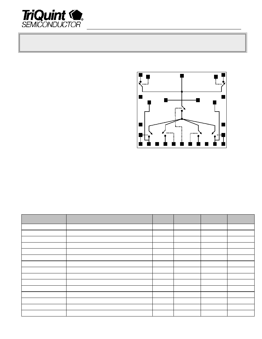
Schematic
Layout:
∑ Unpackaged PHEMT GaAs MMIC Die
∑ Excellent Harmonic Performance
≠80 dBc 2
nd
Harmonic at 1GHz / +34dBm
≠81 dBc 2
nd
Harmonic at 2GHz / +32 dBm
∑ Low Control Voltage Operation to +2.0V
∑ High Tx to Rx Isolation: -40dB typ
∑ Low Insertion Loss: Tx Path 0.45dB typ at 1 GHz
∑ Very Low Control Current: 40 µA Typ
∑ Flexible Bonding Options
Application:
∑ Quad Band for GSM Handset Antenna Switch
Modules (ASM) and Front End Modules (FEM)
∑
Dual and Tri-Band GSM Capable
Description:
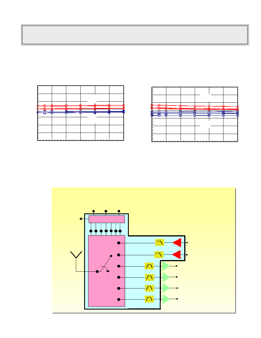
TriQuint's TQ4M4006 is a high power antenna switch die in a single pole six throw (SP6T) configuration. The die
utilizes TriQuint's PHEMT MMIC switch process to provide optimized performance for use in GSM Quad Band
Modules. PHEMT Switches are a very low DC current replacement for classic PIN diode based switches . The die
is ideally suited to applications where the antenna of a GSM headset is to be routed to the two separate Tx ports
and up to four separate Rx inputs. Use of 2 or 3 of the Rx ports allows the same switch die to be used in dual and
tri-band GSM applications. The TQ4M4006 finds applications in Antenna Switch modules combined with Tx Low
Pass Filters and Rx SAW Filters. It is also suitable for use in Front End PA Modules that integrate PA, CMOS
controller/decoder, and filters together. Robust operation is available with stable harmonic performance down to 2.0
V of control voltage.
Electrical Performance: Ta = 25
∞C, Zo=50 Ohms, Vcontrol = 0V / 2.5V
1
Parameter
Test Conditions
Units
Min
Typ
Max
Tx Insertion Loss
GSM850/900
dB
0.45
Tx Insertion Loss
DCS/PCS
dB
0.5
Rx Insertion Loss
GSM850/900
dB
0.7
Rx Insertion Loss
DCS/PCS
dB
1.0
Isolation Rx to Rx
Rx On
dB
-30
Isolation Tx to Rx
Tx On
dB
-42
Isolation Tx to Tx
Tx On
dB
-32
2
nd
Harmonic
GSM850/900, Pin = +34dBm
dBc
-80
2
nd
Harmonic
DCS/PCS, Pin = +32 dBm
dBc
-81
3
rd
Harmonic
GSM850/900, Pin = +34dBm
dBc
-75
3
rd
Harmonic
DCS/PCS, Pin = +32 dBm
dBc
-73
Return Loss
0.5 to 2.0GHz
dB
-20
Leakage Current
-
µA
100
Trise, TFall
10% to 90% RF , 90% to 10% RF
µS
1
Ton , Toff
50% control to 90% RF, and 50% control to 10% RF
µS
1
ANT
ANT
ANT
GND
VRx1
GND Rx2 VRx2 VMode
Rx3
VRx3
GND
VRx4
GND
Rx4
Rx1
Rx4
VRx4
VRx1
GND
Tx1 VTx1
Rx1
GND
Tx2
VTx2
ANT
ANT
ANT
GND
VRx1
GND Rx2 VRx2 VMode
Rx3
VRx3
GND
VRx4
GND
Rx4
Rx1
Rx4
VRx4
VRx1
GND
Tx1 VTx1
Rx1
GND
Tx2
VTx2
SP6T High Power 2.5V Antenna Switch
Quad-Band GSM850/GSM900/DCS/PCS

TQ4M4006 Preliminary Data Sheet
Copyright © 2003 TriQuint (pdc rev 0.1. 061603)
2
All specifications subject to change without notice
SP6T High Power 2.5V Antenna Switch
Quad-Band GSM850/GSM900/DCS/PCS
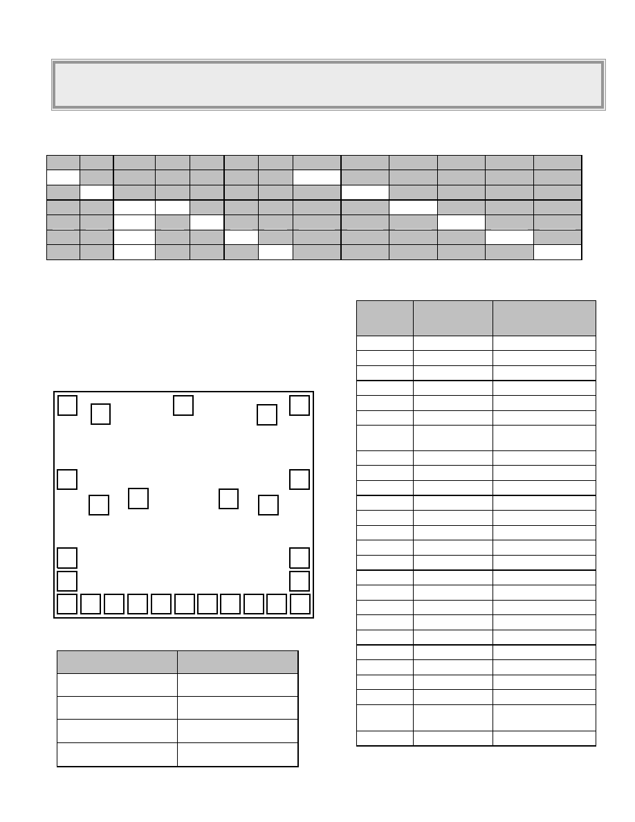
Truth Table:
2, 3
VTx1
VTx2
Vmode
VRx1
VRx2
VRx3
VRx4
ANT-Tx1
ANT-Tx2
ANT-Rx1
ANT-Rx2
ANT-Rx3
ANT-Rx4
1
0
0
0
0
0
0
On
Off
Off
Off
Off
Off
0
1
0
0
0
0
0
Off
On
Off
Off
Off
Off
0
0
1 1 0
0
0
Off
Off
On
Off
Off
Off
0
0
1
0
1
0
0
Off
Off
Off
On
Off
Off
0
0
1
0
0
1
0
Off
Off
Off
Off
On
Off
0
0
1
0
0
0
1
Off
Off
Off
Off
Off
On
Pad
Number
Pad Name
Description
1
Tx1
Transmit RF Port 1
2
VTx1
Control Tx1
3
ANT Main RF ANT Port
4
VTx2
Control Tx2
5
Tx2 Transmit RF Port 2
6
GND
Ground
7 Rx4
Redundant Receive
RF Port 4
8
ANT
Redundant RF ANT
9
GND
Ground
10
VRx4
Redundant Control
11
VRx4
Control Rx4
12
Rx4 Receive RF Port 4
13
GND
Ground
14
Rx3
Receive RF Port 3
15
VRx3
Control Rx3
16
VM
Control TX/RX Mode
17
VRx2
Control Rx2
18
Rx2 Receive RF Port 2
19
GND
Ground
20
Rx1 Receive RF Port 1
21
VRx1
Control Rx1
22
VRx1
Redundant Control
23
GND
Ground
24
ANT
Redundant RF ANT
25 Rx1
Redundant Receive
RF Port 1
26
GND
Ground
Parameter
Absolute Maximum
Max Input Power
+38dBm
Control Voltage
+/-5V
Operating Temp
-40
∞C to +85∞C
Storage Temp
-65
∞C to +150∞C
Absolute Maximum Ratings
4
:
Notes:
1. External DC blocking capacitors are required at all RF ports
2. State 1 = +2.0V to +5.0V, State 0 = 0V to +0.2V
3. Differential voltage from State 1 to State 2 must be a
minimum of 2.0V
4. Exceeding any parameter either individually or in
combination may cause permanent damage.
Die Layout:
ANT
VTx1
Tx1
VTx2
Tx2
GND
Rx4
ANT
ANT
Rx1
Rx1
GND
Rx2
VRx2
VM
VRx3
Rx3
GND
Rx4
VRx4
VRx4
GND
VRx1
VRx1
GND
GND
ANT
VTx1
Tx1
VTx2
Tx2
GND
Rx4
ANT
ANT
Rx1
Rx1
GND
Rx2
VRx2
VM
VRx3
Rx3
GND
Rx4
VRx4
VRx4
GND
VRx1
VRx1
GND
GND

TQ4M4006 Preliminary Data Sheet
Copyright © 2003 TriQuint (pdc rev 0.1. 061603)
3
All specifications subject to change without notice
SP6T High Power 2.5V Antenna Switch
Quad-Band GSM850/GSM900/DCS/PCS
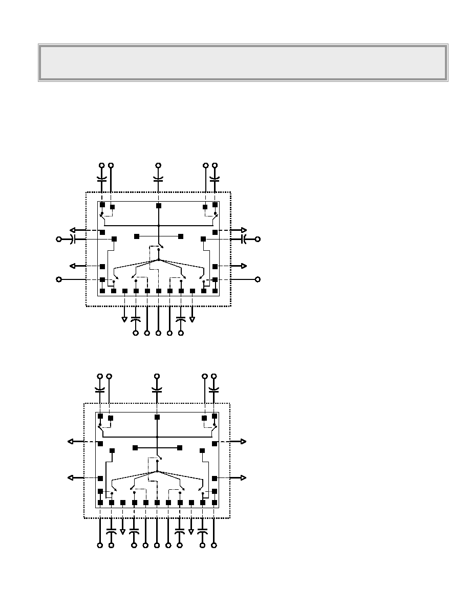
Flexible Bonding Configurations:
External DC Blocking Capacitors are required on all RF ports.
Three Alternate Antenna Bonding Pads
ANT
ANT
ANT
GND
VRx1
GND Rx2 VRx2 VMode
Rx3
VRx3
GND
VRx4
GND
Rx4
Rx1
Rx4
VRx4
VRx1
GND
Tx1 VTx1
Rx1
GND
Tx2
VTx2
ANT
ANT
ANT
GND
VRx1
GND Rx2 VRx2 VMode
Rx3
VRx3
GND
VRx4
GND
Rx4
Rx1
Rx4
VRx4
VRx1
GND
Tx1 VTx1
Rx1
GND
Tx2
VTx2
ANT
ANT
ANT
GND
VRx1
GND Rx2 VRx2 VMode
Rx3
VRx3
GND
VRx4
GND
Rx4
Rx1
Rx4
VRx4
VRx1
GND
Tx1 VTx1
Rx1
GND
Tx2
VTx2
Tx1
ANT
Tx2
Rx1
Rx2
Rx3
Rx4
ANT
ANT
ANT
GND
VRx1
GND Rx2 VRx2 VMode
Rx3
VRx3
GND
VRx4
GND
Rx4
Rx1
Rx4
VRx4
VRx1
GND
Tx1 VTx1
Rx1
GND
Tx2
VTx2
ANT
ANT
ANT
GND
VRx1
GND Rx2 VRx2 VMode
Rx3
VRx3
GND
VRx4
GND
Rx4
Rx1
Rx4
VRx4
VRx1
GND
Tx1 VTx1
Rx1
GND
Tx2
VTx2
ANT
ANT
ANT
GND
VRx1
GND Rx2 VRx2 VMode
Rx3
VRx3
GND
VRx4
GND
Rx4
Rx1
Rx4
VRx4
VRx1
GND
Tx1 VTx1
Rx1
GND
Tx2
VTx2
ANT
Tx1
Tx2
Rx4
Rx3
Rx2
Rx1
ANT
ANT
ANT
GND
VRx1
GND Rx2 VRx2 VMode
Rx3
VRx3
GND
VRx4
GND
Rx4
Rx1
Rx4
VRx4
VRx1
GND
Tx1 VTx1
Rx1
GND
Tx2
VTx2
ANT
ANT
ANT
GND
VRx1
GND Rx2 VRx2 VMode
Rx3
VRx3
GND
VRx4
GND
Rx4
Rx1
Rx4
VRx4
VRx1
GND
Tx1 VTx1
Rx1
GND
Tx2
VTx2
ANT
ANT
ANT
GND
VRx1
GND Rx2 VRx2 VMode
Rx3
VRx3
GND
VRx4
GND
Rx4
Rx1
Rx4
VRx4
VRx1
GND
Tx1 VTx1
Rx1
GND
Tx2
VTx2
ANT
Tx1
Tx2
Rx4
Rx3
Rx2
Rx1
Rx1, Rx4, VRx1 and VRx4
Bonded from Sides
(as used on TriQuint
Application Board)
All Rx Control Lines and Rx Ports
Bonded off Lower Edge

TQ4M4006 Preliminary Data Sheet
Copyright © 2003 TriQuint (pdc rev 0.1. 061603)
4
All specifications subject to change without notice
SP6T High Power 2.5V Antenna Switch
Quad-Band GSM850/GSM900/DCS/PCS
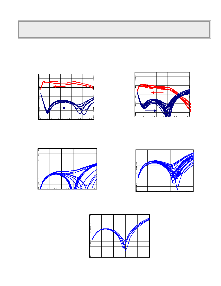
Typical Performance Curves:
SP6T
Tx1 & Tx2 to Antenna (Vctrl=2.5v)
-2.0
-1.8
-1.6
-1.4
-1.2
-1.0
-0.8
-0.6
-0.4
-0.2
0.0
0.0
0.5
1.0
1.5
2.0
2.5
Frequency (GHz)
I
n
sert
i
o
n
L
o
ss (
d
B)
-40
-35
-30
-25
-20
-15
-10
-5
0
5
10
R
e
tu
r
n
L
o
s
s
(d
B
)
SP6T
Rx1 - Rx4 to Antenna (Vctrl=2.5v)
-2.0
-1.8
-1.6
-1.4
-1.2
-1.0
-0.8
-0.6
-0.4
-0.2
0.0
0.0
0.5
1.0
1.5
2.0
2.5
Frequency (GHz)
Ins
e
r
t
i
on Los
s
(
d
B
)
-40
-35
-30
-25
-20
-15
-10
-5
0
5
10
Ret
u
rn
L
o
ss
(
d
B
)
Tx Insertion Loss
Rx Insertion Loss
SP6T
Tx to Rx Isolation Tx on (Vctrl=2.5v)
-60
-55
-50
-45
-40
-35
-30
-25
-20
0.0
0.5
1.0
1.5
2.0
2.5
Frequency (GHz)
Isolation (dB)
SP6T
Rx to Rx Isolation Rx on (Vctrl=2.5v)
-60.0
-55.0
-50.0
-45.0
-40.0
-35.0
-30.0
-25.0
-20.0
0.0
0.5
1.0
1.5
2.0
2.5
Frequency (GHz)
Isolation (dB)
SP6T
Tx to Tx Isolation Tx on (Vctrl=2.5v)
-60.0
-55.0
-50.0
-45.0
-40.0
-35.0
-30.0
-25.0
-20.0
0.0
0.5
1.0
1.5
2.0
2.5
Frequency (GHz)
Isolation (dB)
Isolation Curves

TQ4M4006 Preliminary Data Sheet
Copyright © 2003 TriQuint (pdc rev 0.1. 061603)
5
All specifications subject to change without notice
SP6T High Power 2.5V Antenna Switch
Quad-Band GSM850/GSM900/DCS/PCS
SP6T
Tx1 & Tx2 (F=1.0GHz Pin=34 dBm)
40
50
60
70
80
90
100
110
2.0
2.5
3.0
3.5
4.0
4.5
5.0
Control Voltage (Volts)
Harmonics (dBc)
H2
H3
SP6T
Tx1 & Tx2 (F=2.0GHz Pin=32 dBm)
40
50
60
70
80
90
100
110
2.0
2.5
3.0
3.5
4.0
4.5
5.0
Control Voltage (Volts)
Harmonics (dBc)
H2
H3
1GHz 2
nd
and 3
rd
Harmonics
2 GHz 2
nd
and 3
rd
Harmonics
Application Example:
Quad Band EGSM/GSM850/DCS/PCS
V1 V2 V3 VM V4 V5 V6
SP6T SWITCH
Decoder
Tx/Rx Hi/Lo Band US/Euro
Vcc
DCS/PCS TX
DCS RX
Antenna
GSM850/EGSM TX
PA
TX
PA
TX
GSM850 RX
PCS RX
EGSM RX
LNA
LNA
RX
RX
LNA
RX
LNA
RX
Quad Band EGSM/GSM850/DCS/PCS
V1 V2 V3 VM V4 V5 V6
V1 V2 V3 VM V4 V5 V6
SP6T SWITCH
Decoder
Tx/Rx Hi/Lo Band US/Euro
Vcc
Decoder
Tx/Rx Hi/Lo Band US/Euro
Vcc
Decoder
Tx/Rx Hi/Lo Band US/Euro
Vcc
DCS/PCS TX
DCS RX
Antenna
GSM850/EGSM TX
PA
TX
PA
TX
GSM850 RX
PCS RX
EGSM RX
LNA
LNA
RX
RX
LNA
RX
LNA
RX
DCS/PCS TX
DCS RX
Antenna
GSM850/EGSM TX
PA
TX
PA
TX
GSM850 RX
PCS RX
EGSM RX
LNA
LNA
RX
RX
LNA
RX
LNA
RX
DCS/PCS TX
DCS RX
Antenna
GSM850/EGSM TX
PA
TX
PA
TX
PA
TX
PA
TX
TX
PA
TX
PA
TX
GSM850 RX
PCS RX
EGSM RX
LNA
LNA
RX
RX
LNA
RX
LNA
RX
LNA
LNA
RX
RX
LNA
RX
LNA
RX

TQ4M4006 Preliminary Data Sheet
Copyright © 2003 TriQuint (pdc rev 0.1. 061603)
6
All specifications subject to change without notice
SP6T High Power 2.5V Antenna Switch
Quad-Band GSM850/GSM900/DCS/PCS
100pF Capacitors (7 Places)
Murata GRP1555C1H101JD01
or equivalent
ANTENNA
TX1
RX1
RX2
TX2
RX4
RX3
100pF Capacitors (7 Places)
Murata GRP1555C1H101JD01
or equivalent
ANTENNA
TX1
RX1
RX2
TX2
RX4
RX3
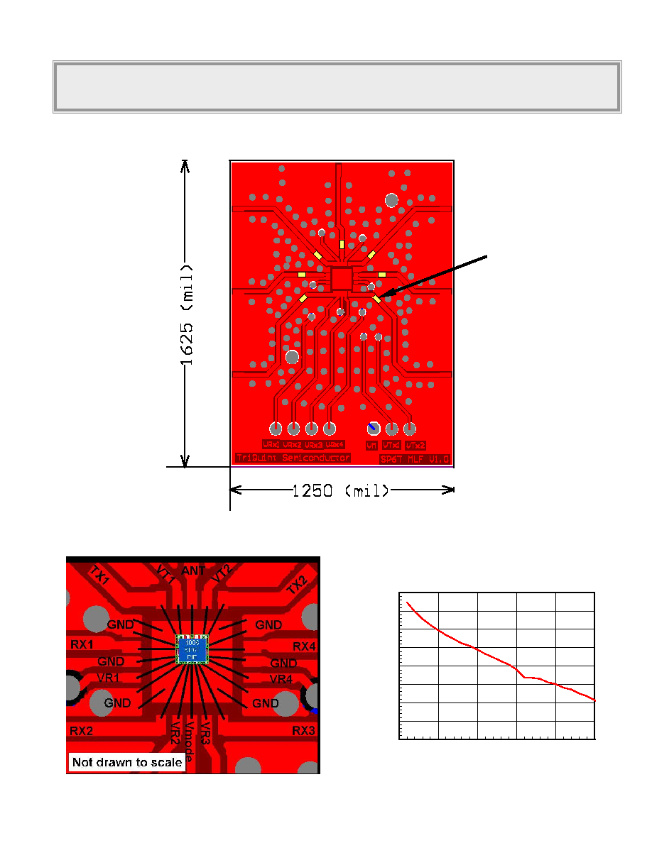
Application Board:
Bonding Configuration:
SP6T TQ4M4006 Samples
Application Board Loss (input + output)
-0.8
-0.7
-0.6
-0.5
-0.4
-0.3
-0.2
-0.1
0.0
0.0
0.5
1.0
1.5
2.0
2.5
Frequency (GHz)
Board Loss (dB)
Application Board Loss De-Embedding Curve:

TQ4M4006 Preliminary Data Sheet
Copyright © 2003 TriQuint (pdc rev 0.1. 061603)
7
All specifications subject to change without notice
SP6T High Power 2.5V Antenna Switch
Quad-Band GSM850/GSM900/DCS/PCS
Additional Information
For latest specifications, additional product information, worldwide sales and distribution locations, and information
about TriQuint:
Web: www.triquint.com
Tel: (503) 615-9000
Email: info_wireless@tqs.com
Fax: (503) 615-8902
For technical questions and additional information on specific applications:
Email:
info_wireless@tqs.com
The information provided herein is believed to be reliable; TriQuint assumes no liability for inaccuracies or
omissions. TriQuint assumes no responsibility for the use of this information, and all such information shall be
entirely at the user's own risk. Prices and specifications are subject to change without notice. No patent rights or
licenses to any of the circuits described herein are implied or granted to any third party.
TriQuint does not authorize or warrant any TriQuint product for use in life-support devices and/or systems.
Copyright © 2003 TriQuint Semiconductor, Inc. All rights reserved.
Revision 0.1 June 16, 2003
For additional information and latest specifications, see our website: www.triquint.com
