 | –≠–ª–µ–∫—Ç—Ä–æ–Ω–Ω—ã–π –∫–æ–º–ø–æ–Ω–µ–Ω—Ç: TQ5635 | –°–∫–∞—á–∞—Ç—å:  PDF PDF  ZIP ZIP |

WIRELESS COMMUNICATIONS DIVISION
For additional information and latest specifications, see our website:
www.triquint.com
1
GND
GND
RF In
GND
LNA
Bias
MXR In
IF Out
GIC
GND
LO
In
GND/LNA
Gain
LNA Out
LO
Vdd
Mixer
Vdd
LNA Vdd
Mixer
IF Amp
LO Buffer
1
active
bias
LNA
GND/LNA
Gain
Active
Bias
TQ5635
DATA SHEET
3 V PCS LNA/Mixer
Receiver IC
Features
?? Single 3.0 V Operation
?? Adjustable Gain/IP3/Current
?? Low Current Operation
?? Few external components
?? QFN 3x3 mm, 16 Pin Leadless Plastic
Package
?? High Input IP3
?? Low Noise Figure
Applications
?? PCS band CDMA mobile Applications
?? Wireless data applications
Product Description
The TQ5635 is an LNA-Downconverter optimized for use in the Korea CDMA
PCS bands. The integrated LNA has a single high gain mode that provides over
15 dB of gain, and features very low NF and excellent IP3. An external resistor
controls LNA bias, making LNA Idd adjustable. The integrated mixer features
very high IP3 and provision for external adjustment of gain, IP3, and Idd.
Because of the external LO tuning inductor, IF's in the range of 85 to 200Mhz
can be used. The excellent RF performance with low current coupled with very
small lead-less plastic package is ideally suited for PCS band mobile phone.
Electrical Specifications
1
Parameter
Min
Typ
Max
Units
RF Frequency
1855
MHz
Conversion Gain
24.5
dB
Noise Figure
2.3
dB
Input 3
rd
Order Intercept
-4.75
dBm
DC supply Current
23.4
mA
Note 1. Test Conditions: Vdd=+2.8V, T
C
=+25C, RF=1855MHz, RF in =-30dBm LO=1635MHz,
LO input=-4dBm, IF=220MHz
2. Data includes image reject filter (Sawtek P/N: 356083) insertion loss of 1.7 dB

TQ5635
Data Sheet
2
For additional information and latest specifications, see our website:
www.triquint.com
Absolute Maximum Ratings
Parameter
Symbol
Minimum
Nominal
Maximum
Units
Storage Temperature
T
store
-40
25
125
deg. C
Case Temperature w/bias
T
c
-40
25
85
deg. C
Supply Voltage
VDD
0
2.8
5.0
V
Voltage to any non supply pin
-
-
-
-
VDD+0.5V
Power Dissipation
P
-
-
100
mW
Signal Power
Ps
-
-
20
dBm
Note 1. All voltages are measured with respect to GND (0V), and they are continuous.
2. Absolute maximum ratings as detailed in this table, are ratings beyond which the device's performance may be impaired and/or permanent damage may occur.
Typical Electrical Characteristics ≠Korea PCS band, Cascade
Parameter
Conditions
Min.
Typ/Nom
Max.
Units
RF Frequency
1840
1870
MHz
IF Frequency
220
MHz
LO input level
2
-7
-4
-1
dBm
Supply voltage
2.8
V
Conversion Gain
1,3,4
21.5
24.5
dB
Noise Figure
1,4
2.3
2.8
dB
Input 3
rd
Order Intercept
1,3,4
-6.5
-4.75
dBm
Supply Current
2,3
23.4
25.0
mA
Note 1.
Test Conditions (devices screened for Conversion Gain, Noise Figure, and IIP3 to the above limits): Vdd = +2.8V, RF = 1855MHz, LO = 1635MHz, IF =
220MHz, LO input = -4dBm, RF input = -30dBm, T
C
= +25
?
C, unless otherwise specified.
2. Min./Max. limits are at +25
?
C case temperature unless otherwise specified.
3.
Conversion Gain and Idd depends on the values of the two resistors used in the GIC circuit and LNA Bias resistor.
4.
Data includes image reject filter (Sawtek P/N: 356083) insertion loss of 1.7 dB

TQ5635
Data Sheet
For additional information and latest specifications, see our website:
www.triquint.com
3
Typical Electrical Characteristics ≠ Korea PCS band, LNA only:
Parameter
Conditions
Min.
Typ/Nom
Max.
Units
RF Frequency
1840
1870
MHz
Conversion Gain
1,3
17.5
dB
Noise Figure
1
1.8
dB
Input 3
rd
Order Intercept
1,3
1.1
dBm
Supply Current
3
7.0
mA
Note 1. Test Conditions: Vdd = +2.8V, RF = 1855MHz, LO = 1635MHz, IF = 220MHz, LO input = -4dBm, RF input = -30dBm, T
C
= +25
?
C, unless otherwise specified.
2. Min./Max. limits are at +25
?
C case temperature unless otherwise specified.
3.
Conversion Gain and Idd depends on the values of the Bias resistor.
Typical Electrical Characteristics ≠ Korea PCS band, Mixer only:
Parameter
Conditions
Min.
Typ/Nom
Max.
Units
RF Frequency
1840
1870
MHz
IF Frequency
220
MHz
Conversion Gain
1,3
9.1
dB
Noise Figure
1
8.2
dB
Input 3
rd
Order Intercept
1,3
11.6
dBm
Supply Current
3
16.5
mA
Note 1: Test Condition: Vdd = +2.8V, RF = 1855MHz, LO = 1635MHz, IF = 220MHz, LO input = -4dBm, RF input = -30dBm, T
C
= +25
?
C, unless otherwise specified..
2. Min./Max. limits are at +25
?
C case temperature unless otherwise specified.
3.
Conversion Gain and Idd depends on the values of the two resistors used in the GIC circuit.
4. Data includes image reject filter (Sawtek P/N: 356083) insertion loss of 1.7 dB

TQ5635
Data Sheet
4
For additional information and latest specifications, see our website:
www.triquint.com
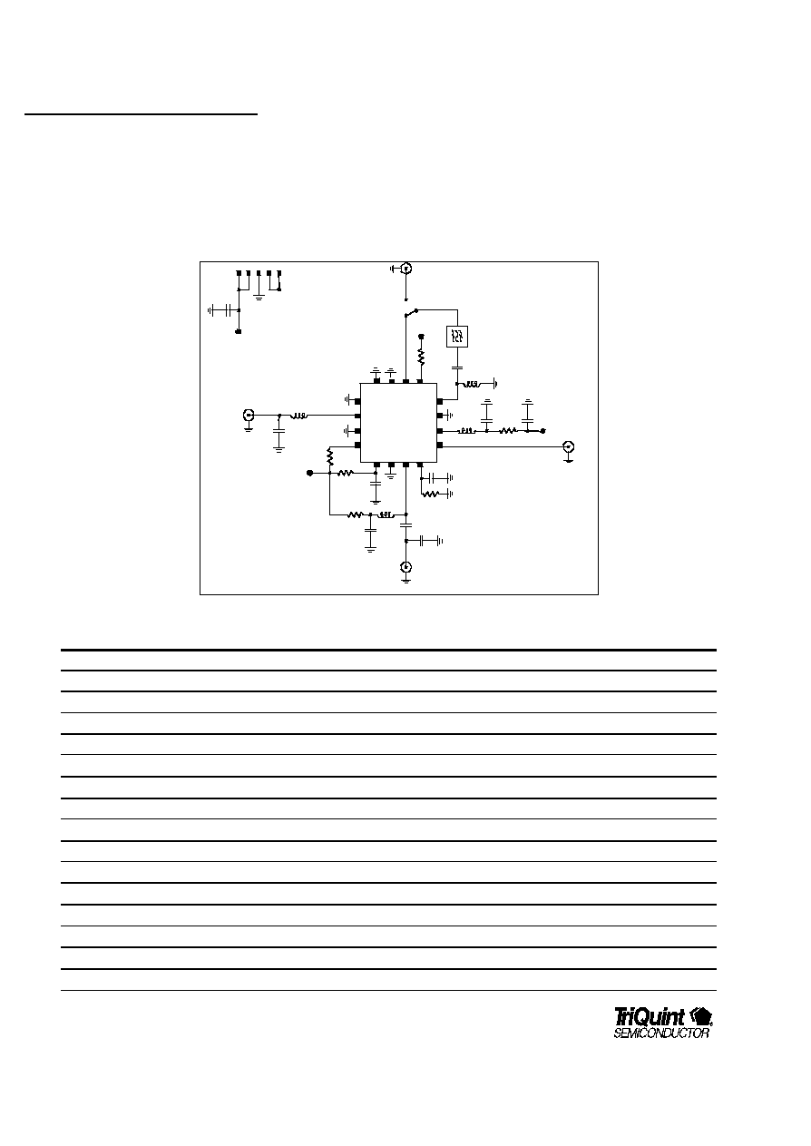
Typical Test Circuit for CDMA KPCS:
Test Conditions (Unless Otherwise Specified): Vdd = +2.8V, RF = 1855MHz, LO = 1635MHz, IF = 220MHz, LO input = -4dBm, RF input = -30dBm, T
C
= +25
?
C
Bill of Material for TQ5635 LNA/Downconverter Mixer for GIC tuning plots
Component
Reference Designator
Part Number
Value
Size
Manufacturer
Receiver IC
TQ5635
3x3mm
TriQuint Semiconductor
Capacitor
C11, C13
0.1uF
0402
Capacitor
C5
2.2pF
0402
Capacitor
C6
1.0pF
0402
Capacitor
C7
1000pF
0402
Capacitor
C8, C9, C10,C13
1000pF
0402
Capacitor
C14
15pF
0402
Capacitor
C15
12pF
0402
Inductor
L1
3.9nH
0402
Coil Craft
Inductor
L2
5.6nH
0402
TOKO
Inductor
L3
56nH
0603
TOKO
Inductor
L4
3.3nH
0402
TOKO
Resistor
R8, R16
3.3O
0402
Resistor
R6
20O
0402
Resistor
R7
* LNA Bias
2.7KO
0402
TQ5635
GND
GND
RF In
GND
LNA
Bias
MXR
In
IF Out
IF Bias
GND
LO
I n
GND
LNA Out
V
DD
MX V
DD
V
DD
LNA Mode
RFin
LOin
AUXin
IFout
Vdd
Vdd
Vdd
C11
L1
C5
R7
R9
C9
R16
C13
L3
C15
C14
C10
R12
L 2
C7
R6
L4
C6
C8
F 1
NC
B+
RL 021401
TOKO
TOKO
0603
Vdd
R8

TQ5635
Data Sheet
For additional information and latest specifications, see our website:
www.triquint.com
5
Resistor
R9
1.8O
0402
Resistor
R12
* GIC
39O
0402
RF Saw Filter
F1
856083
2x2mm
SAWTEK
CDMA KPCS Band
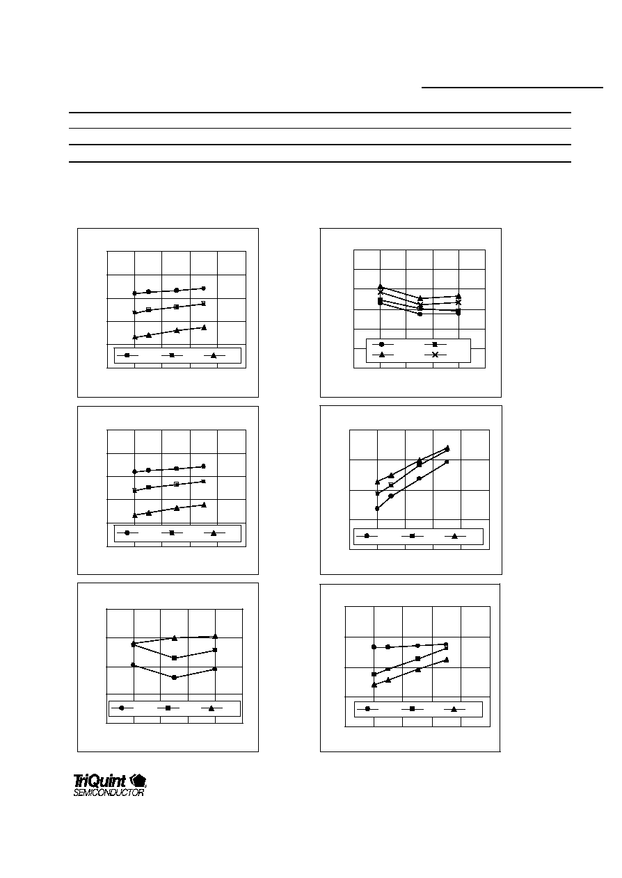
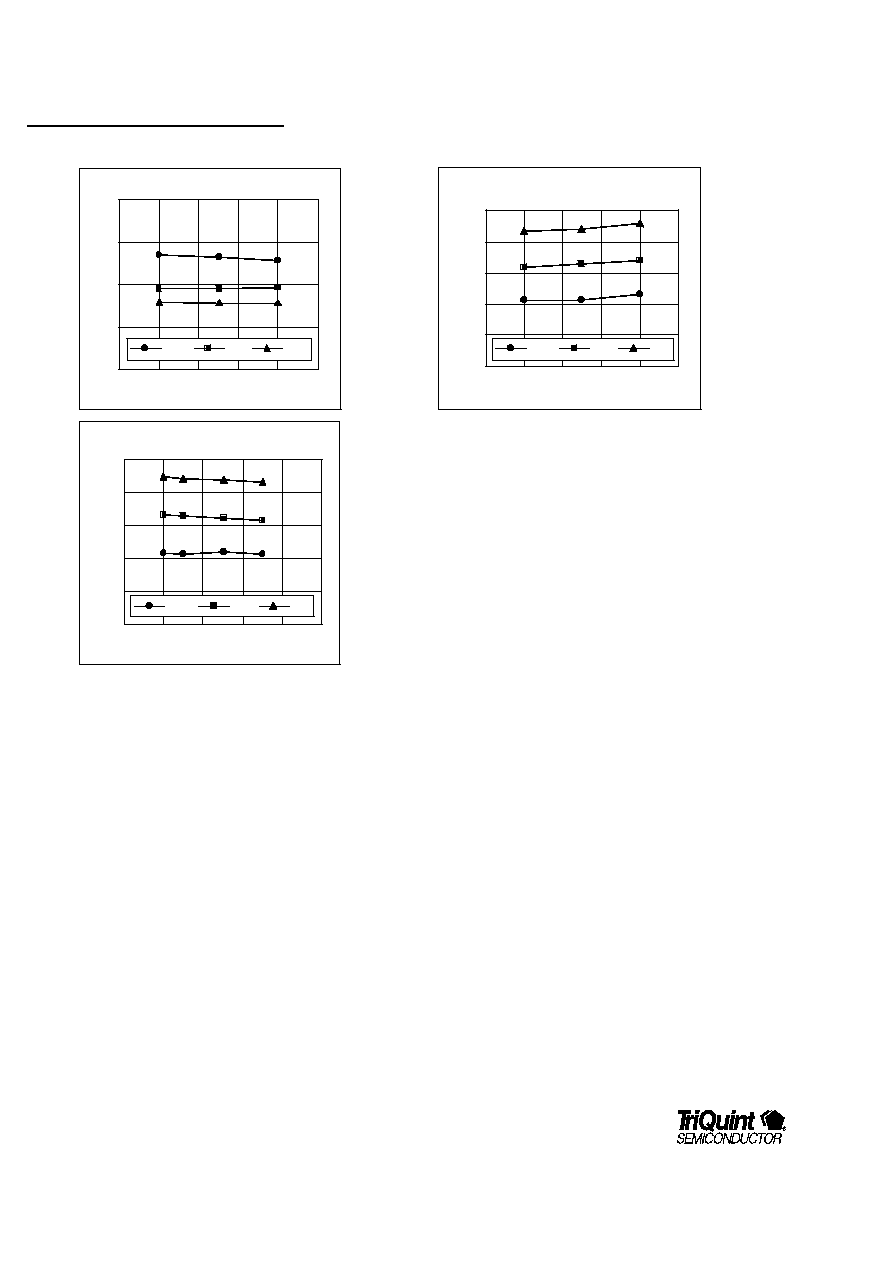
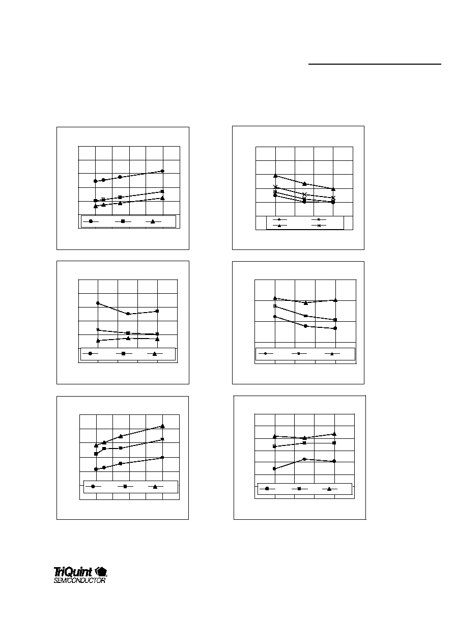
Typical LNA Performance
Test Conditions (Unless Otherwise Specified): Vdd=+2.8V, Tc=+25C, RF = 1852MHz, LO = 1635MHz, I F = 220MHz
Conversion Gain vs Vdd vs Temp
15
16
17
18
19
20
2.5
2.7
2.9
3.1
3.3
3.5
Vdd (V)
Conversion Gain (dB)
-40C
25C
85C
Conversion Gain vs Vdd vs Freq
16
16.5
17
17.5
18
18.5
19
1830
1840
1850
1860
1870
1880
RF Freq (MHz)
Conversion Gain (dB)
2_7V
2_8V
3_2V
3V
Conversion Gain vs Vdd vs Temp
15
16
17
18
19
20
2.5
2.7
2.9
3.1
3.3
3.5
Vdd (V)
Conversion Gain (dB)
-40C
25C
85C
Input IP3 vs Vdd vs Temp
-1
0
1
2
3
2.5
2.7
2.9
3.1
3.3
3.5
Vdd (V)
IP3 (dBm)
-40C
25C
85C
Input IP3 vs Temperature vs Freq
0
0.5
1
1.5
2
1830
1840
1850
1860
1870
1880
RF Freq (MHz)
IP3 (dBm)
-40C
25C
85C
Idd vs Vdd vs Temperature
5
6
7
8
9
2.5
2.7
2.9
3.1
3.3
3.5
Vdd (V)
Idd (mA)
-40C
25C
85C

TQ5635
Data Sheet
6
For additional information and latest specifications, see our website:
www.triquint.com
Idd vs Temperature vs Frequency
5
6
7
8
9
1830
1840
1850
1860
1870
1880
RF Freq (MHz)
Idd (mA)
-40C
25C
85C
Noise Figure vs Temp vs Frequency
0.5
0.9
1.3
1.7
2.1
2.5
1830
1840
1850
1860
1870
1880
RF Freq (MHz)
Noise Figure (dB)
-40C
25C
85C
Noise Figure vs Vdd vs Temp
0.5
0.9
1.3
1.7
2.1
2.5
2.5
2.7
2.9
3.1
3.3
3.5
Vdd (V)
Noise Figure (dB)
-40C
25C
85C

TQ5635
Data Sheet
For additional information and latest specifications, see our website:
www.triquint.com
7
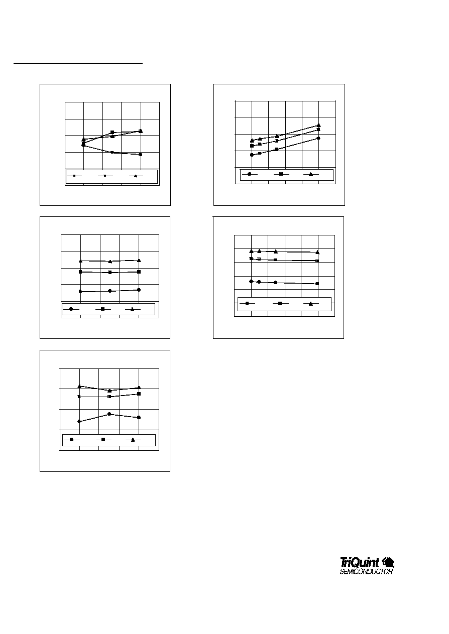
CDMA KPCS Band
Typical Mixer Performance
Test Conditions (Unless Otherwise Specified): Vdd=+2.8V, Tc=+25C, RF = 1852MHz, LO = 1635MHz, I F = 220MHz, LO input = -
4dBm
Gain vs Vdd vs Temperature
7
8
9
10
11
12
13
2.5
2.7
2.9
3.1
3.3
3.5
3.7
Vdd (V)
Conversion Gain (dB)
-40C
25C
85C
Gain vs Vdd vs Frequency
8
8.5
9
9.5
10
10.5
11
1830
1840
1850
1860
1870
1880
RF Freq (MHz)
Conversion Gain (dB)
2_7V
2_8V
3_5V
3V
Gain vs Temperature vs Frequency
7
8
9
10
11
12
13
1830
1840
1850
1860
1870
1880
RF Freq (MHz)
Conversion Gain (dB)
-40C
25C
85C
Conversion Gain vs LO vs Freq
8
8.5
9
9.5
10
1830
1840
1850
1860
1870
1880
RF Freq (MHz)
Conversion Gain (dB)
-1dBm
-4dBm
-7dBm
Input IP3 vs Vdd vs Temperature
8
9
10
11
12
13
14
2.5
2.7
2.9
3.1
3.3
3.5
3.7
Vdd (V)
IP3 (dBm)
-40C
25C
85C
Input IP3 vs Temp vs Frequency
7
8
9
10
11
12
13
14
1830
1840
1850
1860
1870
1880
RF Freq (MHz)
IP3 (dBm)
-40C
25C
85C

TQ5635
Data Sheet
8
For additional information and latest specifications, see our website:
www.triquint.com
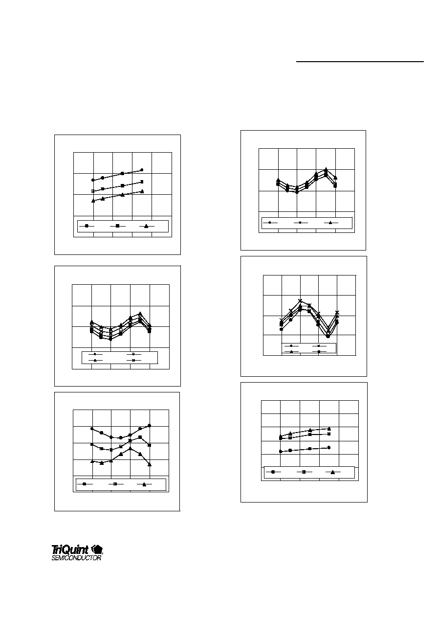
Input IP3 vs LO Drive vs Frequency
10.3
10.7
11.1
11.5
11.9
12.3
1830
1840
1850
1860
1870
1880
RF Freq (MHz)
IP3 (dBm)
-1dBm
-4dBm
-7dBm
Idd vs Vdd vs Temperature
12
14
16
18
20
22
2.5
2.7
2.9
3.1
3.3
3.5
3.7
Vdd (V)
Idd (mA)
-40C
25C
85C
Idd vs Temperature vs Frequency
14
15
16
17
18
19
1830
1840
1850
1860
1870
1880
RF Freq (MHz)
Idd (mA)
-40C
25C
85C
Noise Figure vs Vdd vs Temp
4
5
6
7
8
9
10
2.5
2.7
2.9
3.1
3.3
3.5
3.7
Vdd (V)
Noise Figure (dB)
-40C
25C
85C
Noise Figure vs Temp vs Frequency
3
5
7
9
11
1830
1840
1850
1860
1870
1880
RF Freq (MHz)
Noise Figure (dB)
-40C
25C
85C

TQ5635
Data Sheet
For additional information and latest specifications, see our website:
www.triquint.com
9
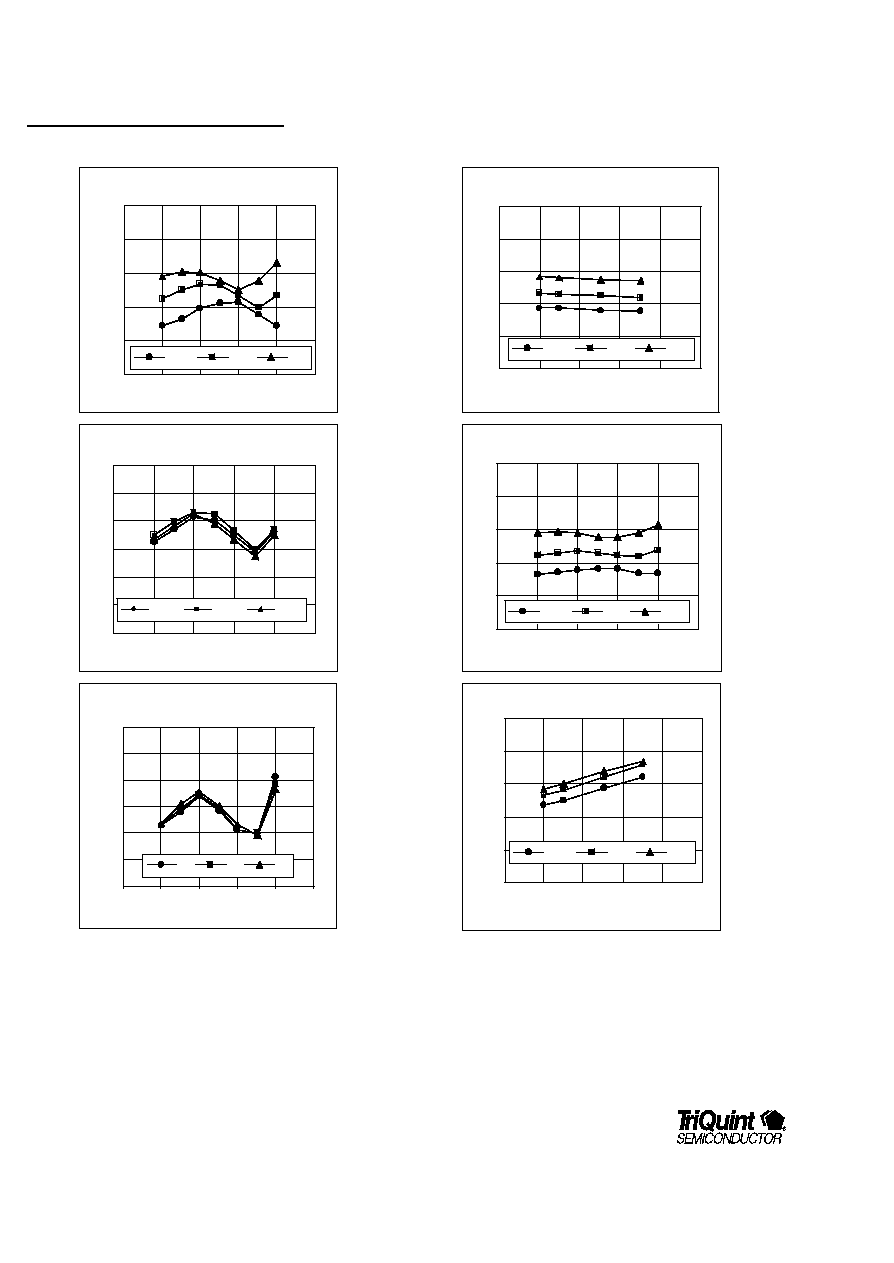
CDMA KPCS Band
Typical Cascade Performance
Test Conditions (Unless Otherwise Specified): Vdd=+2.8V, Tc=+25C, RF = 1852MHz, LO = 1635MHz, I F = 220MHz, LO input = -4dBm
Gain vs Vdd vs Temperature
20
22
24
26
28
2.5
2.7
2.9
3.1
3.3
3.5
Vdd (V)
Conversion Gain (dB)
-40C
25C
85C
Gain vs Vdd vs Frequency
21
23
25
27
29
1830
1840
1850
1860
1870
1880
RF Freq(MHz)
Conversion Gain (dB)
2_7V
2_8V
3_2V
3V
Gain vs Temperature vs Frequency
19
21
23
25
27
29
1830
1840
1850
1860
1870
1880
RF Freq (MHz)
Conversion Gain (dB)
-40C
25C
85C
Gain vs LO vs Frequency
20
22
24
26
28
1830
1840
1850
1860
1870
1880
RF Freq (MHz)
Conversion Gain (dB)
-1dBm
-4dBm
-7dBm
IIP3 vs Vdd Vs Frequency
-7
-6
-5
-4
-3
1830
1840
1850
1860
1870
1880
Frequency (MHz)
IIP3 (dBm)
2_7
2_8
3
3_2
IP3 vs Vdd vs Temperature
-8
-7
-6
-5
-4
-3
-2
2.5
2.7
2.9
3.1
3.3
3.5
Vdd (V)
IP3 (dBm)
-40C
25C
85C

TQ5635
Data Sheet
10
For additional information and latest specifications, see our website:
www.triquint.com
IP3 vs Temperature vs Freq
-10
-8
-6
-4
-2
0
1830
1840
1850
1860
1870
1880
RF Freq (MHz)
IP3 (dBm)
-40C
25C
85C
IP3 vs LO Drive vs Frequency
-9
-8
-7
-6
-5
-4
-3
1830
1840
1850
1860
1870
1880
RF Freq (MHz)
IP3 (dBm)
-1dBm
-4dBm
-7dBm
Noise Figure vs LO vs Frequency
2
2.1
2.2
2.3
2.4
2.5
2.6
1830
1840
1850
1860
1870
1880
Frequency (MHz)
Noise Figure (dB)
-1
-4
-7
Noise Figure vs Vdd vs Temp
0
1
2
3
4
5
2.5
2.7
2.9
3.1
3.3
3.5
Vdd (V)
Noise Figure (dB)
-40C
25C
85C
Noise Figure vs Temp vs Freq
0
1
2
3
4
5
1830
1840
1850
1860
1870
1880
RF Freq (MHz)
Noise Figure (dB)
-40C
25C
85C
Idd vs Vdd vs Temperature
18
20
22
24
26
28
2.5
2.7
2.9
3.1
3.3
3.5
Vdd (V)
Idd (mA)
-40C
25C
85C

TQ5635
Data Sheet
For additional information and latest specifications, see our website:
www.triquint.com
11
Idd vs Temperature vs Frequency
20
21
22
23
24
25
26
1830
1840
1850
1860
1870
1880
RF Freq (MHz)
Idd (mA)
-40C
25C
85C

TQ5635
Data Sheet
12
For additional information and latest specifications, see our website:
www.triquint.com
Pinout Description:
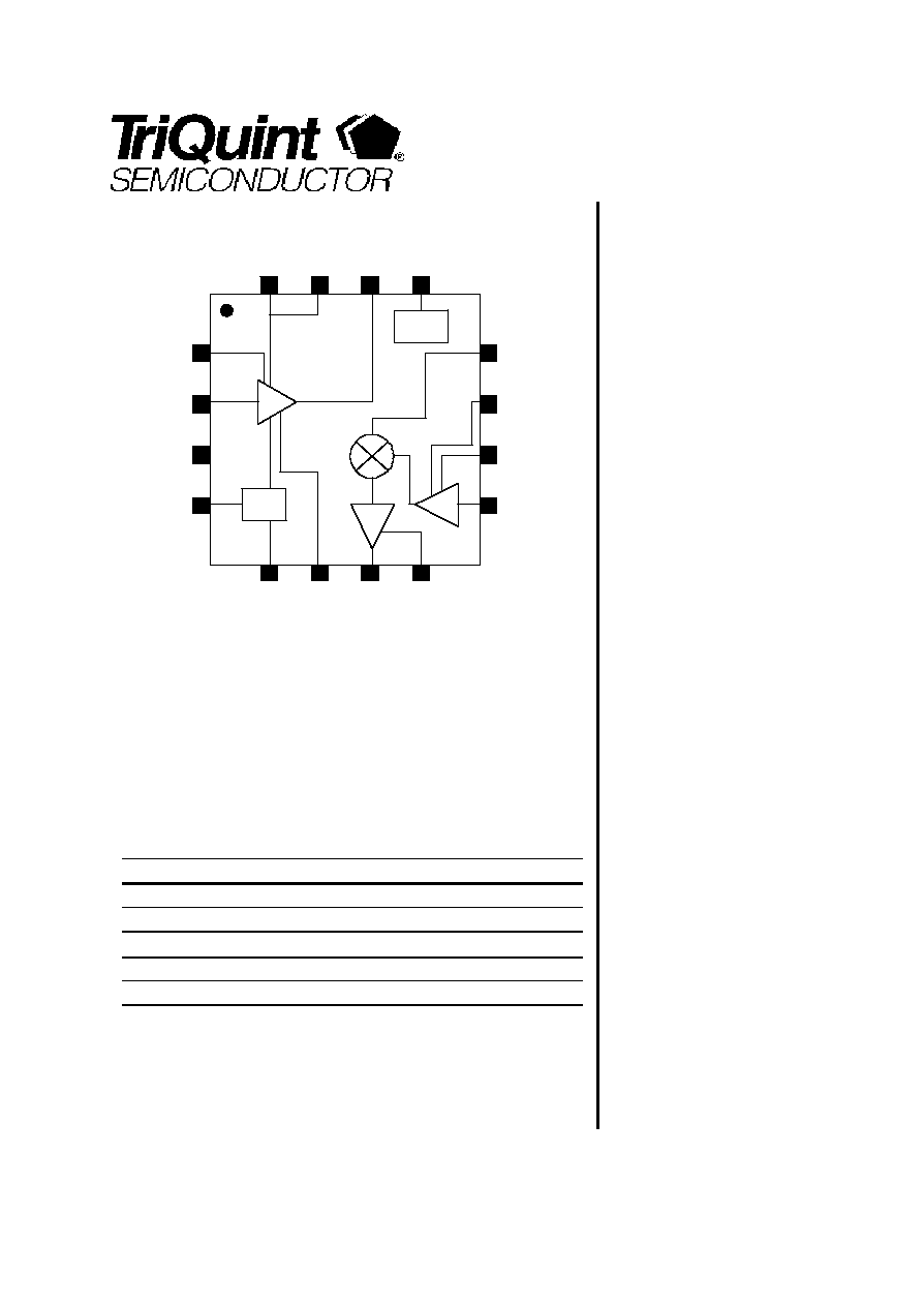
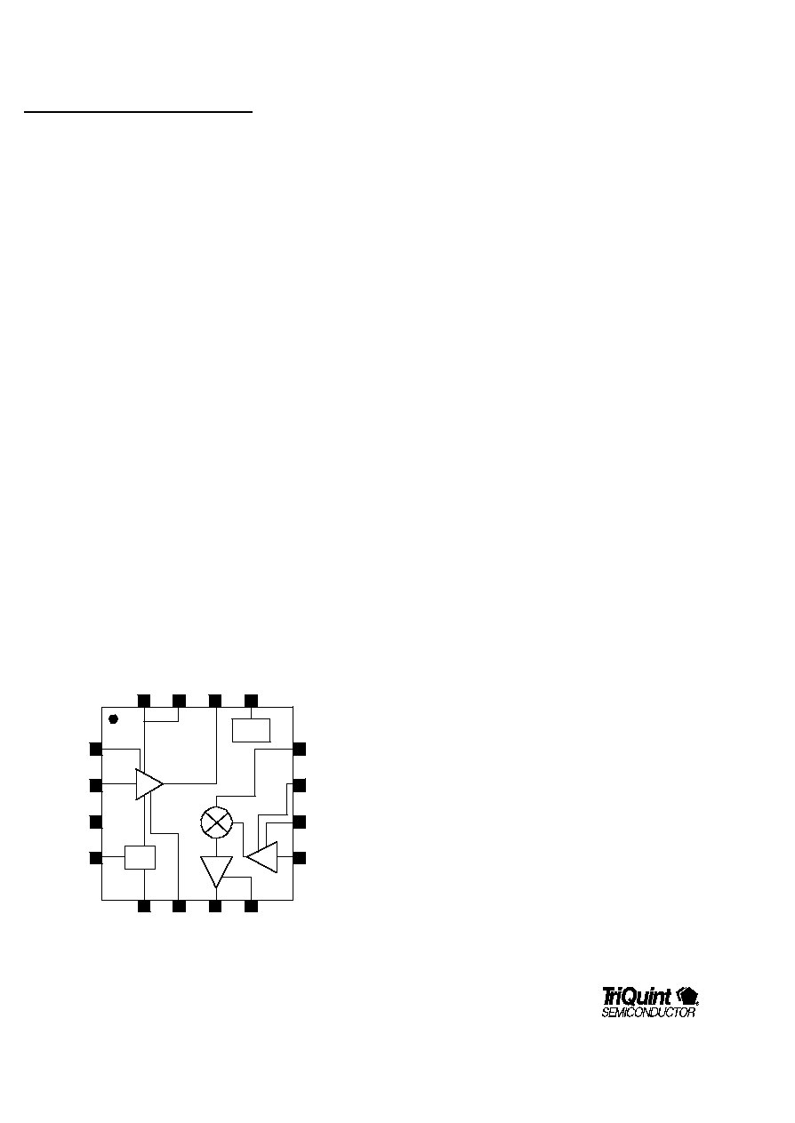
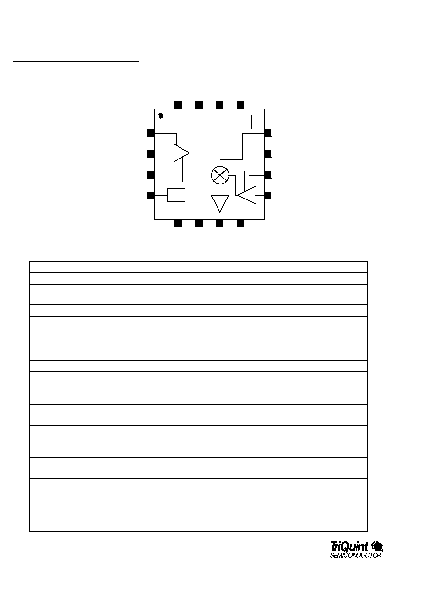
The TQ5635 is a complete front-end for a Korea high
band CDMA handset receiver. It combines a high IP3
low noise amplifier, a high intercept mixer, and an IF
amplifier.
The LNA uses an off-chip matching network which connects to
the input at pin 2. The amplifier was designed so that the
match for maximum gain also gives very low noise figure.
The LNA has a single high gain mode that typically provides
15-16dB of gain.
The LNA also provides several ways of setting gain and
intercept in the design phase. The LNA FET source is
brought out to Pins 15 and 16, where a small value of
inductance to ground can be added. The inductor can be
discrete or simply a small length of pc board trace. Several
dB of adjustment is possible. For most applications,
maximum gain will be desired. In that case, pins 15 and 16
should be connected to ground with multiple vias. A bias
resistor on pin 4 is used to set the LNA supply current. A
nominal value of 2.7kohm is recommended.
The LNA output signal is at Pin 14. It is a 50 ohm line and can
be connected directly to a SAW image filter. The image filter
output connects to the mixer input at Pin 12. The mixer
receives its LO via a buffer which amplifies the signal from Pin
9. The buffer transistor drain comes out of Pin 10 where it
connects to an external LO tuning inductor.
GND
GND
RF In
GND
LNA
Bias
MXR In
IF Out
GIC
GND
LO
I n
GND/LNA
Gain
LNA Out
LO
Vdd
Mixer
Vdd
LNA Vdd
Mixer
IF Amp
LO Buffer
1
active
bias
LNA
GND/LNA
Gain
Active
Bias
Figure 1. TQ5635 Block diagram
The IF signal from the mixer is fed to an amplifier. The IF
amplifier is an open drain type with output at Pin 7. An
external matching circuit is required to match the IF output to
a filter. The IF amplifier also has a GIC pin (Gain-Intercept-
Current). It is used to set the DC current and gain of the IF
stage.
Application Information:
Half IF Spur Rejection Considerations:
The TQ5635 has a single ended mixer so Half-IF spur
rejection is set by the image filter. Thus we do not
recommend using an IF that is less than 2.5 times the image
filter.
Grounding:
With good layout techniques there should not be any stability
problems. Poor circuit board design can result in a circuit that
oscillates. Good grounding is especially important for the
TQ5635 since it uses an outboard LO tuning inductor that
provides one more potential ground loop path. One could
use the evaluation board as an example of proper layout
techniques.
It is important to position the LO tuning, GIC, and IF matching
components as close to the chip as possible. If the
components are far enough away they and their
corresponding pc board traces can act as quarter wave
resonators in the 5-10Ghz region. If both the IF and the LO
paths to ground resonate at the same frequency, oscillation
can result.
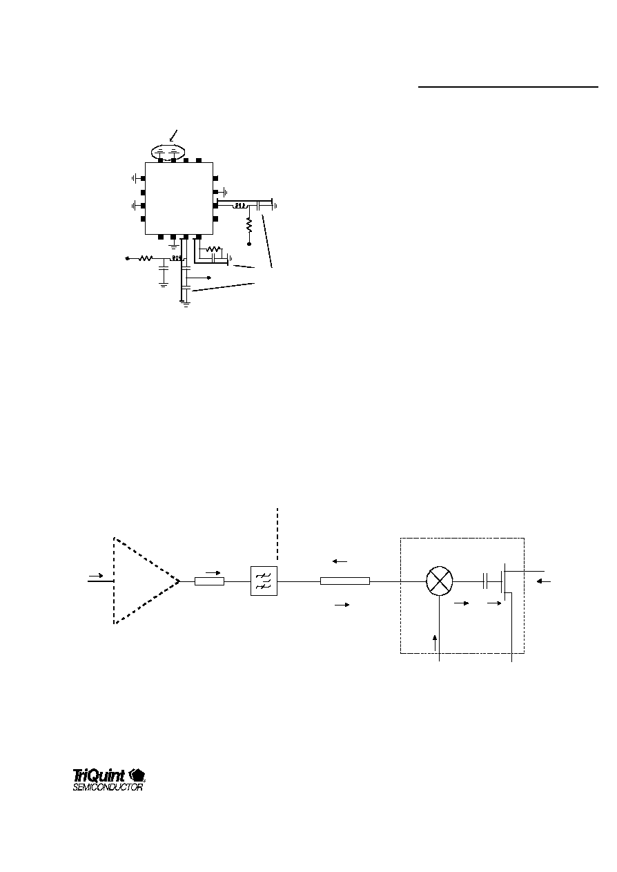
It is most important that the ground on the GIC bypass cap,
the ground on the LO tuning bypass capacitor, and the IF
shunt cap ground return back to the chip grounds with minimal
inductance (Figure 2).
Also, improving the ground at the LO tuning inductor bypass
cap will increase circuit Q. Thus mixer drive is improved with
a resultant higher IP3. Improved ground here means minimal
inductance between the chip ground pins and the other
ground return points. Although it is not a stability issue,
proper grounding of pins 15 and 16 is necessary for maximum
LNA gain. Multiple vias to ground should be placed very close
to those pins.

TQ5635
Data Sheet
For additional information and latest specifications, see our website:
www.triquint.com
13
Vdd
Vdd
IFout
Minimize These
Lengths
TQ5635
GND
GND
RF In
GND
LNA
Bias
MXR
In
IF Out
IF Bias
GND
LO
In
GND
LNA Out
V
DD
V
DD
V
DD
GND
Use multiple ground vias for
maximum LNA gain
Figure 2. Critical signal Paths
Mixer ≠ Filter Interaction:
Before attempting a new TQ5635 application, it is important to
understand the nonlinear interaction between the image filter
and the mixer subcircuit. The device IP3 is a strong function
of this interaction. For this reason it is helpful to consider the
filter and mixer as one nonlinear block.
Figure 3 shows a much simplified block diagram of the LNA,
image filter, and mixer. The RF signal is amplified by the
LNA, passes through the image filter, and is converted down
to the IF where it is amplified by the IF output FET. The
quiescent current in the IF amplifier is set by the GIC network.
Both the filter and the mixer terminate the RF signal with
50ohms.
However, the situation is much different with the LO signal. At
the LO frequency the image filter looks like a short circuit.
Some LO energy leaks out of the mixer input, bounces back
off of the image filter and returns back into the mixer with
some phase or delay. The delayed LO signal mixes with the
normal LO to create a DC offset in the passive FET. A DC
blocking capacitor prevents the offset voltage from affecting IF
stage current.
It has been found empirically that varying the delay between
the filter and mixer can have positive or negative
consequences on IP3, CG, and NF. It is for this reason that
an LC network is useful between the SAW and mixer input,
even though the mixer input can have an adequate match at
the RF frequency without any external components.
25-100 ohms at RF-
short circuit at LO
band pass
LO Leakage
LO Leakage
??????
Mixer
LO
IF
RF in
Mixer Portion
of TQ5635
+ LO) = DC Offset
(LO Leakage
?????
at Mixer IF Output
Mixer in
12
9
LNA Out
2
14
LNA Portion
of TQ5635
Idd
IF Output
FET
to GIC
IF Output
8
7
IF + DC
Offset
Blocking Cap
Figure 3. Non-linear filter-Mixer Interaction

TQ5635
Data Sheet
14
For additional information and latest specifications, see our website:
www.triquint.com
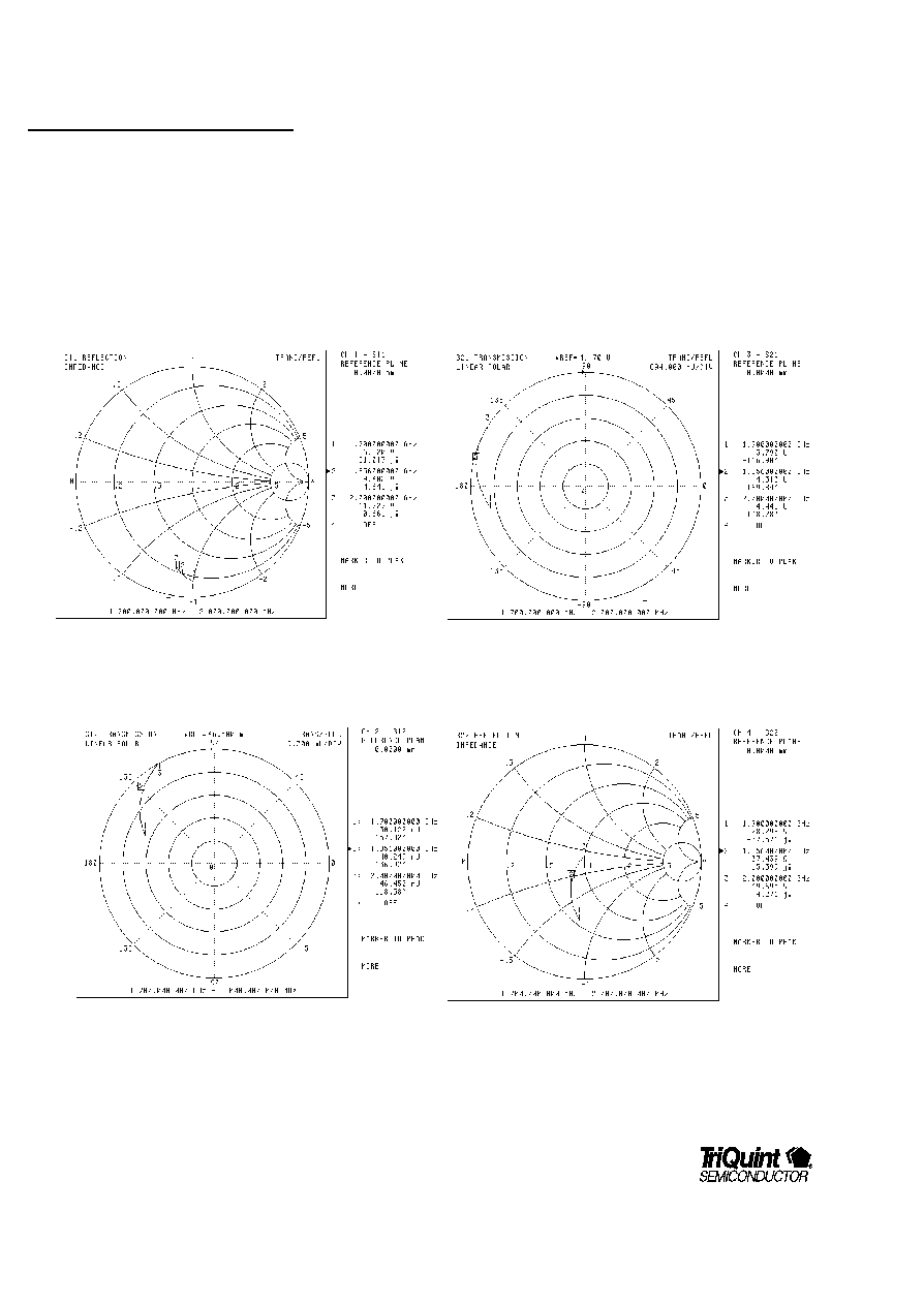
LNA S-Parameters :
S-Parameters for the TQ5635 LNA taken in the high mode. We have not included noise parameters since for this device Gamma-Opt
is very close to the conjugate match.
Figure 4: LNA S11
Figure 5: LNA S12
Figure 6: LNA S21
Figure 7: LNA S22

TQ5635
Data Sheet
For additional information and latest specifications, see our website:
www.triquint.com
15
SUGGESTED STEPS FOR TQ5635 TUNING:
The following order of steps is recommended for applying the
TQ5635. They are described in detail in the following sections:
Lay out board consistent with the grounding guidelines at the
beginning of this note. See section 1 regarding LNA source
inductor.
1. Determine the LNA bias resistor value and source inductor
value
2. Determine the LNA input matching network component
values. Test the LNA by itself.
3. For the mixer, experimentally determine proper LO tuning
components. This step needs to be done first since all of the
later tuning is affected by it.
4. Determine a tentative GIC network. It will have to be fine-
tuned later, since the image filter interaction will affect device
current.
5. Synthesize a tentative IF output match. It may have to be
fine-tuned later, as the final GIC configuration affects IF stage
current. LO is turned ON.
6. Experimentally determine a tentative mixer RF Input match.
LO is turned ON. Test the filter-mixer cascade. Verify that
the device has adequate IP3. If not, another RF Input
matching topology can be tried.
7. Fine tune GIC components for needed Idd. LO is turned ON.
8. Check IF match to see if it still is adequate. LO is turned ON.
9. Test the device as a whole - LNA, filter, mixer
1. Determine LNA Bias Resistor Value and Source Inductor
Value
For most designs we recommend an LNA bias resistor of 2.7K
ohms. All of the datasheet specs assume that value of resistor.
However, if LNA Idd < 7.5 mA is desired, then the resistor can
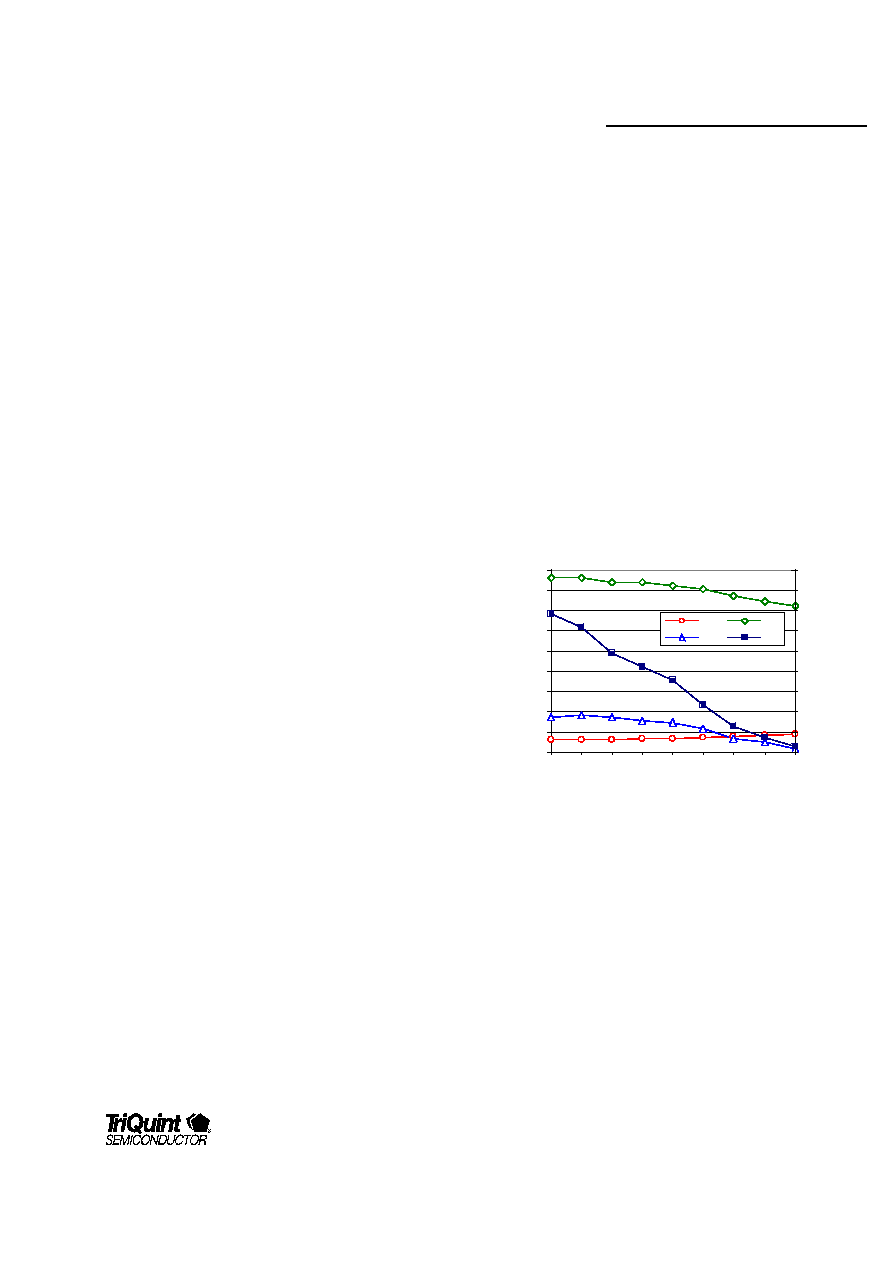
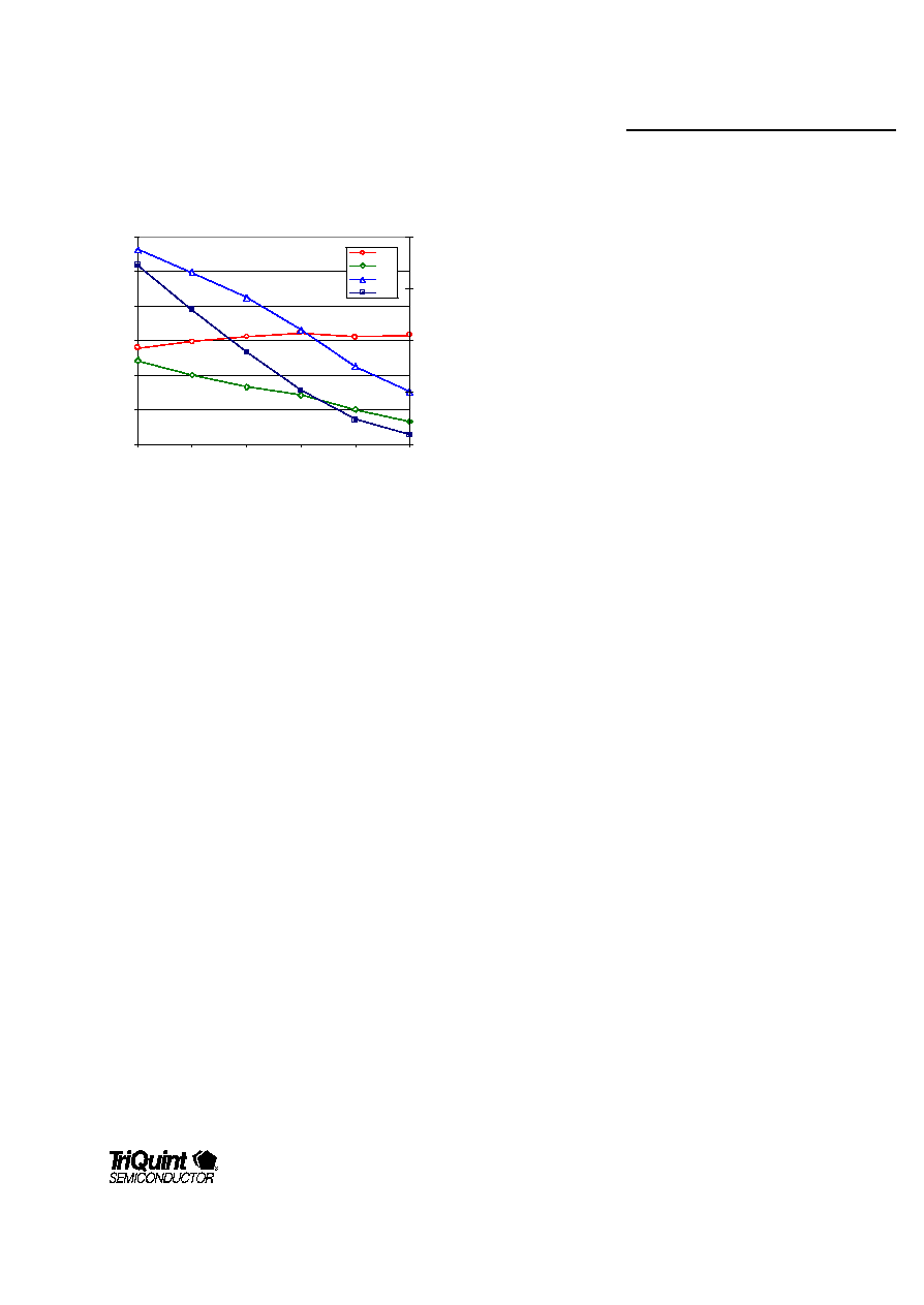
be made larger. Refer to Figure 8 for graphs of LNA
performance vs. bias resistor.
Please keep in mind that there are implications of reduced LNA
bias that are not reflected in IP3. For example, the LNA is
normally in front of the image filter so that it may need
resistance to blocking or other types of distortion that are not
adequately described by the IP3 figure of merit.
Figure 8: Gain, IIP3, Idd, and NF as a Function of Rbias
5635 LNA
NF, Gain, IIP3 and Idd vs bias
resistor
0
2
4
6
8
10
12
14
16
18
1.1
1.5
2.2
2.7
3.3
4.7
6.8
8.2
1 0
Bias resistor (kOhms)
dB
3
4
5
6
7
8
9
1 0
1 1
1 2
Idd (mA)
NF
Gain
IIP3
Idd

TQ5635
Data Sheet
16
For additional information and latest specifications, see our website:
www.triquint.com
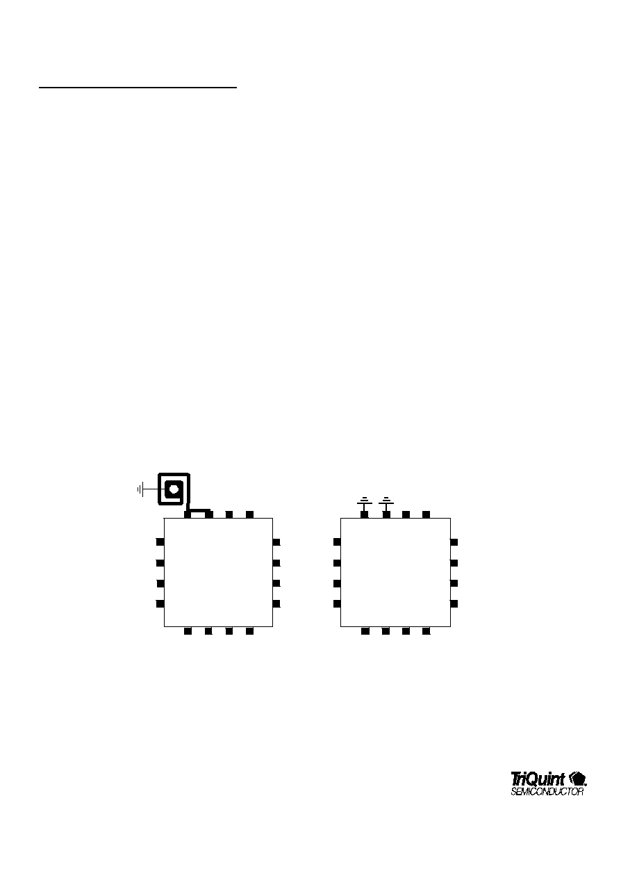
For most applications needing maximum LNA gain, it
will probably be sufficient to simply ground pins 15
and 16 as shown in the second diagram in Figure 9.
However, in some cases a small amount of
inductance may be needed from pins 15 and 16 to
ground in order to lower the LNA gain. Because of
stray inductance on the application board layout, it is
difficult to give a precise value of L as a function of
gain reduction. The first diagram in Figure 9
illustrates one way of doing this. A short is placed
across the inductor until the needed gain is arrived at.
2. Determine the LNA Matching Network
Matching network design for the TQ5635 LNA is much
simpler than designing with discrete transistors. The
TQ5635 LNA was designed so that the optimum noise
match is very close to the conjugate match. Thus
once a match to 50ohms is attained, only a slight
adjustment to the L and C values may be needed for
optimum noise figure. If the design uses 5-8mil
dielectric FR4 board, then it is likely that the
component values on the evaluation board can be
used for a starting point. Alternately, a network can
be synthesized from the S-parameter values at the
end of this note.
3. LO Buffer Tuning
The drain of the LO buffer is brought out to pin 10
where it is fed DC bias via an inductor. The inductor
resonates with the internal and external parasitic
capacitance associated with that pin. For maximum
performance the resonance must be at or near the
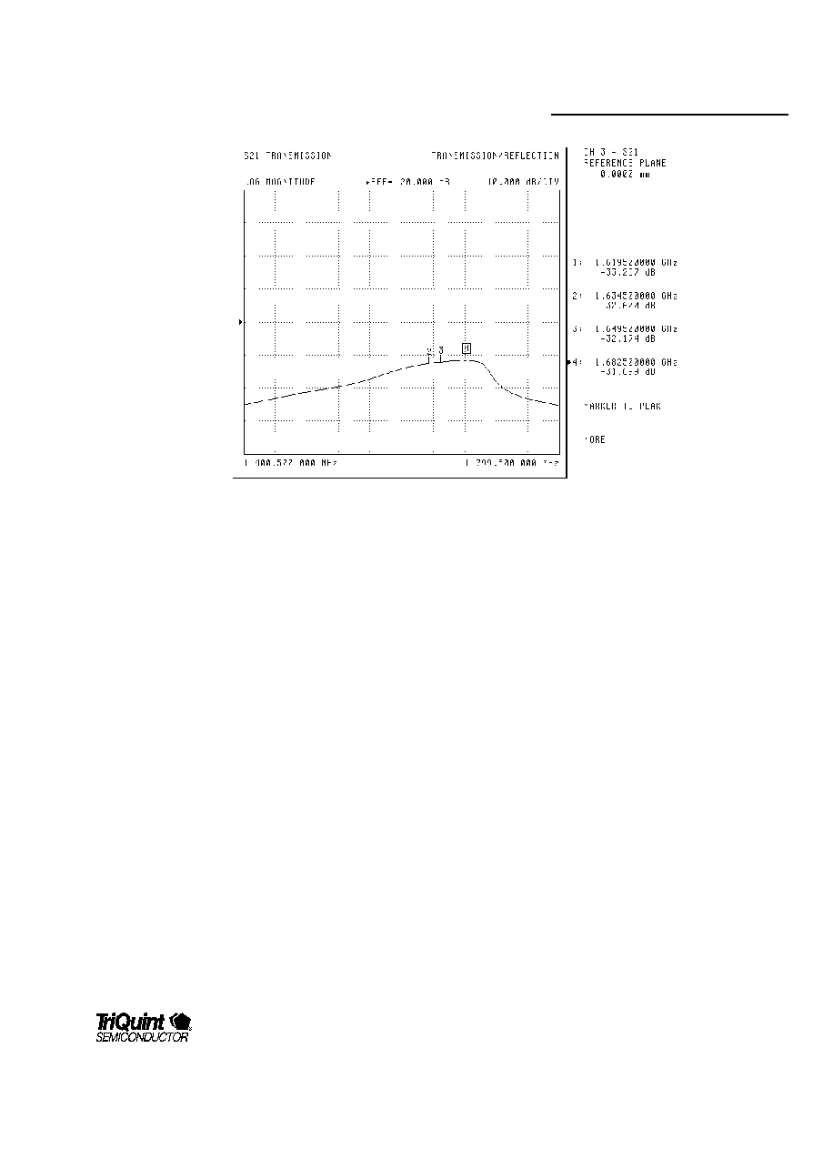
desired LO frequency. Figure 10 shows a properly
tuned LO buffer. Notice that the LO frequency range
of interest is to the left of the peak. We recommend
that the LO is tuned slightly higher in frequency, so
that the desired band is on the lower, more gradual
side of the slope. Thus there is less change in
performance versus frequency. We have also found
empirically that tuning the LO slightly higher in
frequency results in much better LO input and RF
input matches.
TQ5635
GND
GND
RF In
GND
LNA
Bias
MXR
In
IF Out
IF Bias
GND
LO
In
GND
LNA Out
V
DD
V
DD
V
DD
TQ5635
GND
GND
RF In
GND
LNA
Bias
MXR
In
IF Out
IF Bias
GND
LO
In
GND
LNA Out
V
DD
V
DD
V
DD
GND
GND
Recommended: Ground
pins 15 and 16 for
maximum gain
For Lower Gain: add a
small inductance to pins
15 and 16
Figure 9: LNA Source Inductor Realization

TQ5635
Data Sheet
For additional information and latest specifications, see our website:
www.triquint.com
17
Figure 10: Suggested LO Tuning Response
A first approximation to the needed inductor can be found by
the following equation:
1
L = ---------------- - 1nH where C=1.5pF
C (2*pi*F)
2
It is likely that when the design is prototyped, the needed
inductance will fall between two standard inductor values. It is
advised to use a slightly larger inductor and then use the
bypass capacitor for fine tuning. When using this method it is
important to isolate the tuning inductor/bypass cap node from
the Vdd bus, since loading on the bus can affect tuning. A
resistor of 3.3ohm to 20ohm has been found to work well for
this purpose (R2).
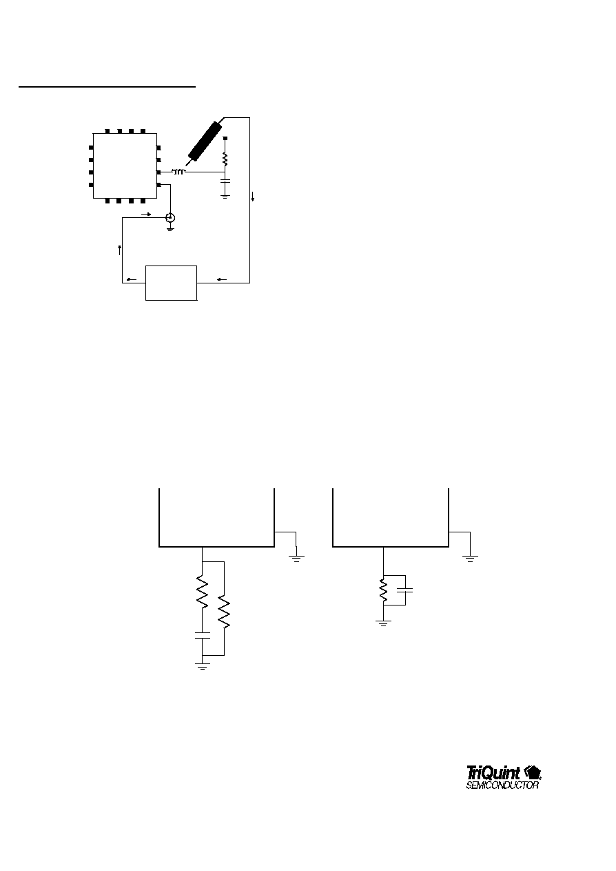
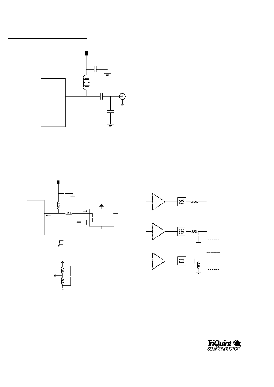
Figure 11 shows the recommended test setup for tuning the
TQ5635 LO buffer. A network analyzer is set to the center of
the LO band +/- 300Mhz, with an output power of ≠4dBm. It is
important to set the frequency range to be quite a bit wider
than the LO band, so that the shape of the tuning curve can
be seen. A two port calibration is performed and the analyzer
is set to monitor S21. Port 1 of the analyzer is connected to
the LO port of the TQ5635, while Port 2 is connected via cable
to a short length of semi-rigid coaxial probe. The center of the
probe should protrude 1 to 2 mm beyond the ground shield.
The end of the probe with the exposed center conductor is
held close to the LO tuning inductor.

TQ5635
Data Sheet
18
For additional information and latest specifications, see our website:
www.triquint.com
LO IN
VDD
NETWORK
ANALYZER
PORT 1
MEASURE S21
COAXIAL
PROBE
TQ5635
GND
GND
RF In
GND
LNA
Bias
MXR
In
IF Out
IF Bias
GND
LO
In
GND
LNA Out
V
DD
V
DD
V
DD
GND
Figure 11: LO Tuning Test Setup
4. GIC Network Design
The GIC pin on the TQ5635 is connected internally to the
source of the IF output stage. By adding one or two resistors
and a capacitor to this pin, it is possible to vary both the IF
stage AC gain, and the IF stage quiescent current. However,
there is a limit to the amo unt of gain increase that is possible,
since there is always some package and bond wire
inductance back to the die. Furthermore, although some
additional IP3 performance may be gained by increasing the
quiescent current, in practice it makes no sense to increase
Idd beyond that which provides maximum input intercept. At
some point IP3 is limited by the mixer FET, and no further
increase in input intercept can be obtained by adjusting the IF
stage.
There are two GIC schemes that are recommended for the
TQ5635 (Figure 12). The first uses a small resistor (1.0 to 5
ohms) in series with a bypass capacitor to set the AC gain.
The IF stage current is then set by the larger resistor (40 to 80
ohms) that connects directly from the GIC pin to ground. The
small degeneration resistor lowers the IF stage gain.
The second scheme, which is recommended for maximum
gain, uses a resistor in parallel with capacitor. The resistor
sets the DC current, while the capacitor bypasses it at the IF
frequency. For highest gain, place the capacitor as close to
Pin 7 as possible. Try to avoid capacitors which are self-
resonant at the IF frequency.
Here is an approximate equation for Rgic as a function of IF
stage Idd: Rgic ~ 0.6 / IDD_IF
GIC PIN
GIC PIN
Chip
GND
Chip
GND
0 to 5 ohms
40 to 80 ohms
40 to 80 ohms
Zc bypass
at IF Freq
Zc bypass
at IF Freq
AC degen
sets IF
current
sets IF
current
Figure 12: GIC Pin Networks

TQ5635
Data Sheet
For additional information and latest specifications, see our website:
www.triquint.com
19
5635 Mixer
NF, Gain, IIP3 and Idd vs GIC resistor
6
7
8
9
10
11
12
47
56
68
82
100
110
GIC resistor (kOhms)
dB
8
10
12
14
16
Idd (mA)
NF
Gain
IIP3
Idd
Figure 13: Mixer Performance as a Function of Rgic
5. IF Match Design
The Mixer IF output (Pin 7) is an "open-drain" configuration,
allowing for flexibility in efficient matching to various filter
types and at various IF frequencies. An optimum lumped-
element-matching network must be designed for maximum
TQ5635 conversion gain and minimum matching network loss.
When designing the IF output matching circuit, one has to
consider the output impedance, which will vary somewhat
depending on the quiescent current and the LO drive. The IF
frequency can be tuned from 45 to 400 MHz by varying
component values of the IF output matching circuit. The IF
output pin also provides the DC bias for the output FET.
In the user's application, the IF output is most commonly
connected to a narrow band SAW or crystal filter with
impedance from 500 -1000
?
with 1 - 2 pF of capacitance. A
conjugate match to a higher filter impedance is generally less
sensitive than matching to 50
?
. When verifying or adjusting
the matching circuit on the prototype circuit board, the LO
drive should be injected at the nominal power level (-4 dBm),
since the LO level does have an impact on the IF port
impedance.
There are several networks that can be used to properly
match the IF port to the SAW or crystal IF filter. The IF FET
bias is applied through the IF output Pin 7, so the matching
circuit topology must contain either a RF choke or shunt
inductor.
For purposes of 50 ohm evaluation, the shunt L, series C,
shunt C circuit shown in Figure 14 is the simplest and requires
the fewest components. DC current can be easily injected
through the shunt inductor and the series C provides a DC
block, if needed. The shunt C, in particular can be used to
improve the return loss and to reduce the LO leakage. The
circuit is used on our evaluation board.
For matching into a filter, the circuit of Figure 15 works well.
The network provides the needed impedance transformation
with a lower loaded Q using reasonable inductor values.
Thus matching circuit loss is minimized. The ratio between
(L1+L2) and L2 is proportional to the square root of the
impedances to be matched, Z1 and Z2. The sum of L1 and
L2 must be chosen so that the total inductance resonates with
the SAW input capacitance. If this resonant frequency is
much higher than the IF frequency, then Copt can be added to
lower it. Please note that because of parasitic capacitance
and the discrete values of commercial inductors, the formulas
of Figure 15 only serve as a starting point for experimentation.
In order to minimize loss, any inductors used should have high
Q. Typically 0805 size inductors perform better than the 0603
size. If 0603 inductors must be used for space
considerations, make certain to use High-Q types. It is
possible to introduce 3dB of additional loss by using low Q
inductors. Additionally, it is recommended to place the IF filter
very close to the TQ5635. If the two are far apart a
transmission line will be needed between them. In that case
two matching networks will be needed, one to match down to
50ohms and one to match back up to 1000ohms. Twice the
loss can be expected for such a scheme.

TQ5635
Data Sheet
20
For additional information and latest specifications, see our website:
www.triquint.com
IF
OUT
Vdd
Cshunt
Cseries
bypass
L
50
ohms
Figure 14: IF Output Match to 50 ohms
IF
OUT
Vdd
L1
C
opt
bypass
L2
IF
SAW
balanced
IF Out
Z1
Z2
C
saw
Equivalent
Circuit
Z 1
Z2
L 2
L1
C
saw
SAW
IF
C
L
L
F
?
?
)
(
4
1
2
1
2
2
?
2
1
2
2
1
L
Z
Z
L
L
?
?
Figure 15: IF Match to a SAW Filter
6. Mixer RF Input Matching Network:
Although the TQ5635 can present <2:1 SWR to the SAW filter
without a matching circuit, it is still recommended to use an
inter-stage network. We have found that the Mixer-Filter
interaction discussed earlier can result in degraded OIP3 at
higher LO power levels with no network. Probably more time
will be needed for this phase of the design than for any other,
since it involves a process of trial-and-error.
For example, the evaluation board network was chosen after
trying all three of the types of Figure 16. For each type, there
was found component L and C values which gave >10dB
return loss at the RF frequency (LO is turned on for this
testing). Then a SAW filter was added in cascade and IP3
was tested. The circuit of Figure 12-C was found to have
superior IP3.
The final test of the filter-network-mixer cascade is to connect
a network analyzer at the SAW input and measure S11 with
the mixer turned on. A 2:1 or better SWR should be seen in
the RF pass band of the SAW. At that point, the filter-
network-cascade is ready to be tested with the LNA.
TQ5635
Mixer
12
12
12
A
B
C
SAW
SAW
SAW
TQ5635
Mixer
TQ5635
Mixer
RF In
TQ5635
LNA
14
2
RF In
TQ5635
LNA
14
2
RF In
TQ5635
LNA
14
2
Figure 16: SAW -Mixer Input Networks

TQ5635
Data Sheet
For additional information and latest specifications, see our website:
www.triquint.com
21
7. Redo GIC Components:
After obtaining the optimum network between the SAW and
Mixer RF input, most likely Idd will have changed slightly.
Determine a new GIC resistor to bring Idd to the desired
value.
8. Double Check IF Match
After any change which affects IF stage current it is importa nt
to recheck the IF output match. This is especially true when
matching down to 50ohms, since the match is more sensitive.
A match to a 1000ohm filter will not be as sensitive. The LO
must be turned ON during the test.
9. Test the TQ5635 Cascade:
Finally after the LNA and Mixer are properly tuned the device
performance as a whole should be measured.

TQ5635
Data Sheet
22
For additional information and latest specifications, see our website:
www.triquint.com
Package Pinout:
GND
GND
RF In
GND
LNA
Bias
MXR In
IF Out
GIC
GND
LO
In
GND/LNA
Gain
LNA Out
L O
Vdd
Mixer
Vdd
LNA Vdd
Mixer
IF Amp
LO Buffer
1
active
bias
LNA
GND/LNA
Gain
Active
Bias
Pin Descriptions:
Pin #
Pin Name
Description and Usage
1
GND
Ground connection. Connect as closely as possible to ground or to package paddle ground.
2
LNA IN
LNA RF input (DC blocked internally). An external match is required which can be chosen for a gain/NF
trade-off.
3
GND
Ground connection. Connect as closely as possible to ground or to package paddle ground.
4
LNA BIAS
An external resistor is connected between this pin and Vdd in order to set the LNA bias current. A value of
~ 2.5 KOhm will give an LNA IDD of ~ 7 mA.
5
LNA VDD
LNA supply voltage. An external decoupling/bypass network should be used.
6
GND
Ground connection. Connect as closely as possible to ground or to package paddle ground.
7
IF OUT
Mixer IF output (~ 500 Ohm, open drain). Connection to Vdd required. External matching required.
8
IF BIAS
IF amp FET source. An RF by -passed resistor is placed form this pin to ground in order to set the current in
this stage.
9
LO IN
Mixer LO input (DC blocked internally). Internally matched to ~ 50 Ohms.
10
LO TUNE
Mixer LO buffer supply voltage. An external bypass capacitor required. An external series inductor is
required for peaking LO gain.
11
GND
Ground connection. Connect as closely as possible to ground or to package paddle ground.
12
MXR IN
Mixer RF input (DC blocked internally). An external matching network is recommended to optimized
cascaded IIP3
13
MXR Vdd
Supply voltage for the internal bias circuit that sets IF amp current (in conjunction with the external IF BIAS
resistor).
14
LNA OUT
LNA RF output. It is DC blocked and internally matched to better than 2:1.
15, 16
LNA SOURCE
The source node of the cascade LNA section. A hard ground provides maximum gain and minimum IIP3. A
small amount of external inductance will reduce gain and improve IIP3.
Paddle
GND
Ground connection. It is very important to place multiple via holes under the paddle. Provides RF
grounding for the part.

TQ5635
Data Sheet
23
For additional information and latest specifications, see our website: www.triquint.com
23
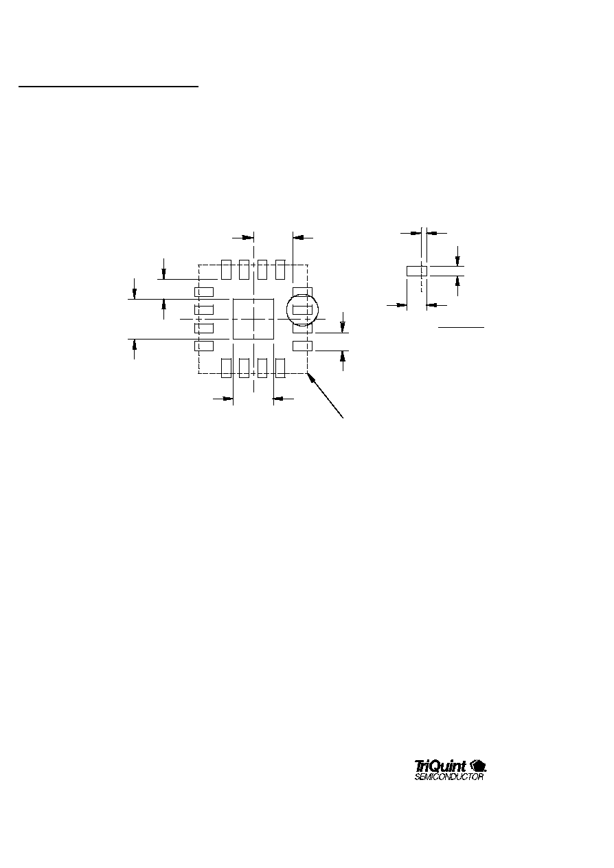
Recommended PC board Layout to Accept 16 Pin Lead-less Plastic Package:
1.10 [0.043]
1.10 [0.043]
1.10 [0.043]
0.13 [0.005]
0.50 [0.020]
PACKAGE OUTLINE
0.25 [0.010]
DETAIL A
0.53 [0.021]
A
0.55 [0.022]
PITCH 4X SIDES
LEADLESS 3x3-16 PCB FOOTPRINT
NOTES:
1. ONLY GROUND SIGNAL TRACES ARE ALLOWED DIRECTLY UNDER THE PACKAGE.
2. PRIMARY DIMENSIONS ARE IN MILLIMETERS, ALTERNATE DIMENSIONS ARE IN INCHES.

TQ5635
Data Sheet
Additional Information
For latest specifications, additional product information, worldwide sales and distribution locations, and information about TriQuint:
Web: www.triquint.com
Tel: (503) 615-9000
Email: info_wireless@tqs.com
Fax: (503) 615-8902
For technical questions and additional information on specific applications:
Email: info_wireless@tqs.com
The information provided herein is believed to be reliable; TriQuint assumes no liability for inaccuracies or omissions. TriQuint assumes no responsibility for the use of
this information, and all such information shall be entirely at the user's own risk. Prices and specifications are subject to change without notice. No patent rights or
licenses to any of the circuits described herein are implied or granted to any third party.
TriQuint does not authorize or warrant any TriQuint product for use in life-support devices and/or systems.
Copyright © 2001 TriQuint Semiconductor, Inc. All rights reserved.
Revision A, February 22, 2001
24
For additional information and latest specifications, see our website:
www.triquint.com
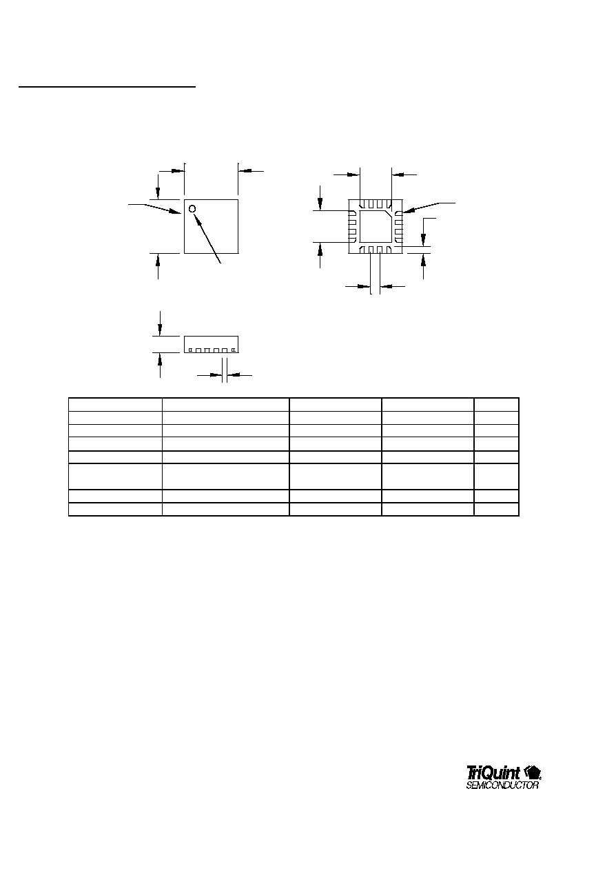
Package Type: QFN 3x3-16 Lead-less Plastic Package
L
D
b
A
E
PIN 1
D2
e
E2
PIN 1
LASER
MARK
PIN 1 ID
JEDEC DESIGNATION DESCRIPTION
METRIC
ENGLISH
Notes
A
OVERALL HEIGHT
0.90 +/-.10 mm
.035 +/-.004 in
1
b
TERMINAL WIDTH
.250 +/-.025 mm
.010 +/-.001 in
1
D
PACKAGE LENGTH
3.00 mm BSC
.118 in
1
D2
EXOPSED PAD LENGTH
1.80 +/-.15 mm
.071 +/-.006 in
1
e
TERMINAL PITCH
.50 mm BSC
.020 in
1
E
PACKAGE WIDTH
3.00 mm BSC
.118 in
1
E2
EXPOSED PAD WIDTH
1.80 +/-.05 mm
.071 +/-.002 in
1
L
TERMINAL LENGTH
.40 +/-.05 mm
.016 +/-.002 in
1
Notes:
1. Primary dimensions are in metric millimeters. The English equivalents are calculated and subject to rounding error.
Additional Information

TQ5635
Data Sheet
25
For additional information and latest specifications, see our website: www.triquint.com
25
For latest specifications, additional product information, worldwide sales and distribution locations, and information about TriQuint:
Web: www.triquint.com
Tel: (503) 615-9000
Email: info_wireless@tqs.com
Fax: (503) 615-8902
For technical questions and additional information on specific applications:
Email: info_wireless@tqs.com
The information provided herein is believed to be reliable; TriQuint assumes no liability for inaccuracies or omissions. TriQuint assumes no responsibility for the use of
this information, and all such information shall be entirely at the user's own risk. Prices and specifications are subject to change without notice. No patent rights or
licenses to any of the circuits described herein are implied or granted to any third party.
TriQuint does not authorize or warrant any TriQuint product for use in life-support devices and/or systems.
Copyright © 2001 TriQuint Semiconductor, Inc. All rights reserved.
