 | –≠–ª–µ–∫—Ç—Ä–æ–Ω–Ω—ã–π –∫–æ–º–ø–æ–Ω–µ–Ω—Ç: TQ8213 | –°–∫–∞—á–∞—Ç—å:  PDF PDF  ZIP ZIP |

T
R
I Q
U
I
N
T
S E M I C O N D U C T O R , I N C .
1
PRELIMINARY DATA SHEET
TELECOM
PRODUCTS
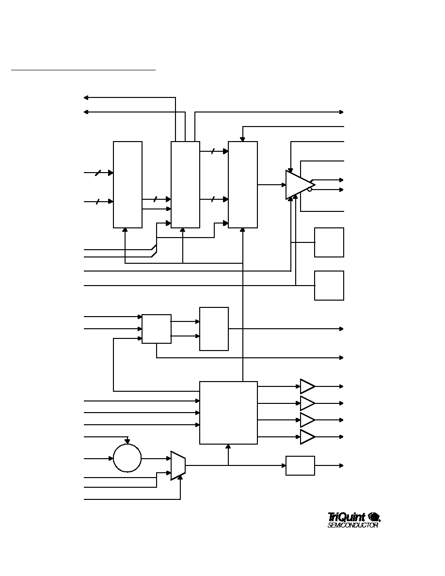
The TQ8213 is a SONET/SDH OC48 MUX that time-division multiplexes a
16-bit or 32-bit parallel data bus to a serial 2.48832 Gb/s NRZ data stream
for transmission through a communications channel. Without any
additional amplification, the 2.48832 Gb/s output stage can drive either a
directly modulated laser or an optical external modulator. Output may also
be configured to provide standard ECL/PECL levels with excellent rise/fall
times. The serial output data stream is available through either single-
ended or differential pins. Mark/space ratio adjustment allows
compensation for asymmetries encountered in optoelectronics.
The TQ8213 operates in two different time-division multiplexing modes,
making it extremely flexible for use in telecom and datacom applications.
The serial 2.48832 Gb/s data stream can be generated from either a 16-bit
wide 155.52 MHz data stream or a 32-bit wide 77.76 MHz data stream.
Data integrity may be ensured through a byte-wise parity check, which
occurs in parallel with the incoming data stream. An external parity alarm
is set whenever a parity check error is detected.
Transmit clocking is selectable from either an internal or external Voltage
Controlled Oscillator(VCO) as well as a selectable external or internal Phase
Locked Loop (PLL). The selected clock source may be monitored at
HCKOUT. The internal PLL utilizes an external reference clock, REFCLK, to
aid in timing generation. The reference clock may be one of seven
commonly used system frequencies. A TTL level LOCK signal is supplied
to indicate when the phase difference between the external reference clock
and the internal divided down clock is less than
/4 radians.
Operating from a single +5V supply, the TQ8213 will provide fully
compliant functionality and performance. Direct-connected TTL levels are
used with both of the input modes.
The TQ8213 is fully compliant with SONET/SDH jitter specifications.
TQ8213
OC48/STM16
Multiplexer
Features
∑ Single-chip 16:1 or 32:1
Multiplexer with integrated clock-
synthesis and high performance
75mA/3.75V output driver
∑ Output can drive external optical
modulator, 50
PECL/ECL
transmission line, or directly
modulated laser without further
amplification
∑ Output symmetry adjust
∑ Selectable internal/external active
highspeed 2.48832 GHz clock
∑ SONET/SDH compliant for
2.48832 Gb/s output data rate
∑ 622.08, 311.04, 155.52, 77.76,
51.84, 38.88, or 19.44 MHz
PECL or TTL reference clock
inputs
∑ Integrated PLL with external filter
∑ Four output clocks at 311.04,
155.52, 77.76, and 38.88 MHz.
∑ Internal even/odd (mode
programmable) parity checker
with alarm output
∑ 23mm 208-pin BGA package
∑ 5V single supply
∑ ≠40 to +125
∞
C case operating
temperature

2
TQ8213
PRELIMINARY DATA SHEET
Figure 1. TQ8213 Block Diagram
TDPERR
PARALM
TD1(0:7)-
TD4(0:7)
TDPAR(1:4)
MODE(0)
MODE(1)
VSYMX
VOSC
REFCLK
VLEVEL
VTUNEIN
NCLKIN
CLKSEL
VDRIVE
VSEN1
DOUT
NDOUT
VTUNEO
VSEN10
LOCK
CK311
CK155
CK78
CK39
HCKOUT
REFSEL0
REFSEL1
REFSEL2
CLKIN
REFCLKT
RESET
PARSEL
TTL
Buffer
32
MUX
Retime
VCO
Internal
VSYMX
Source
Internal
VLEVEL
Source
Clock Divider
1
0
50
Resistive
Tap
2.48832GHz
Clock Input
Selector
Active Clock
Phase
Freq.
Detector
Charge
Pump
4

TQ8213
3
SONET/SDH/A
TM
PRODUCTS
PRELIMINARY DATA SHEET
TELECOM
PRODUCTS
Function Description
Timing Generation
The TQ8213 utilizes an external 2.48832 GHz (nominal)
reference clock, or generates a 2.48832 Ghz clock
through an internal VCO. The active clock can be
monitored on a 50
output, HCKOUT. The active clock
is selected via the CLKSEL pin as shown in the
following table.
CLKSEL
Active Clock
N.C.
External Clock (CLKIN)
VEE
Internal VCO
External Clock VCO and PLL
The external clock, CLKIN and NCLKIN, may be input as
either single-ended (unused input must be externally
terminated through a capacitor to an AC ground) or
differential and must be AC coupled. The external clock
is selected as the active clock if the CLKSEL line is left
open(N.C.). Note VOSC and VTUNEIN must be tied to
VEE when using an external VCO.
Internal Clock VCO and PLL
See Figure 8 for operation with the internal clock and
PLL. The internal clock is selected when CLKSEL is tied
to VEE and the external power supply pin, VOSC, is tied
to VDD. CLKIN must be tied to VEE through a 10k
resistor when the internal clock is used.
The internal PLL is composed of a Phase/Frequency
Detector (PFD), a charge pump, and the internal VCO.
An external system reference clock must be provided at
REFCLK (PECL) or REFCLKT (TTL). The unused
REFCLK or REFCLKT input must be tied to a logic low.
The reference clock can be one of seven different
frequencies. Control pins, REFSEL2, REFSEL1, and
REFSEL0, are set according to the following table when
the corresponding reference clock frequency is used.
REFSEL2 REFSEL1 REFSEL0
REFCLK Freq.
0
0
0
19.44 MHz
0
0
1
38.88 MHz
0
1
0
51.84 MHz
0
1
1
77.76 MHz
1
0
1
155.02 MHz
1
1
0
311.04 MHz
1
1
1
622.08 MHz
The PFD compares the phase between an internal
clock
divided from the active clock and the reference clock at
REFCLK. The PFD's phase error signals are then
integrated by the Charge Pump and external loop filter,
which provides a VCO tune voltage at VTUNEO. See
Table 4 for recommended external loop filter passive
values. The internal PLL is completed by connecting
VTUNEO to VTUNEIN. The internal PLL provides an
active high TTL in-lock indicator at LOCK when the
phase difference between external reference clock and
the internal divided down
clock is less than
/4
radians.
Internal Clock and VCO and External PLL
See Figure 9 for operation with the internal clock and
external PLL. When an external PLL is used an
internally generated clock (such as CK39) and
VTUNEIN can be used in the external PLL.
Output Clocks
The TQ8213 contains an internal Clock Divider block
which frequency divides the active clock (internal or
external source as selected by the CLKSEL). The Clock
Divider supplies the internal clock signals necessary for
the re-timing and multiplexing functions. The Clock
Divider block also outputs four external clocks: a
311.04 MHz differential PECL clock at CK311 and
NCK311, a 155.52 MHz PECL clock at CK155, a 77.76

4
TQ8213
PRELIMINARY DATA SHEET
MHz TTL clock at CK78, and a 38.88MHz PECL clock at
CK39. Note that the above clock frequencies are
dependant upon using the part at 2.48832 GHz.
Data Multiplexing and Parity Checking
The TQ8213 can be configured to run in one of two
modes. The demultiplexing modes are set by fixing the
MODE(1) and MODE(0) package pins according to the
following table.
MODE(1) MODE(0)
Multiplexing Mode
N.C.
VEE
16:1
VEE
N.C.
32:1
VEE
VEE
TBD
Parity mode is programmable by PARSEL. If PARSEL is
left open, the TQ8213 checks for even parity. If PARSEL
is tied to VEE, the TQ8213 checks for odd parity.
For all modes the first output bit in time is TD10. The
remainder of the data is output sequentially from TD11
through TD27. The most significant byte is Byte #1
which is TD10 through TD17.
For 16:1 multiplexing applications, the TQ8212 receives
an 16-bit wide 155.52 MHz data bus at the TD1(0:7)
and TD2(0:7) pins, and two 155.52MHz parity bits at
the TDPAR1 and TDPAR2 pins. The 16-bit wide data
and parity bits are re-timed by an internal 155.52 MHz
clock supplied by the Clock Divider Block. Incoming
data integrity is ensured by a byte-wise parity check
performed internally on the re-timed TD1(0:7) and
TD2(0:7) data with the respective re-timed TDPAR1 and
TDPAR2 parity bits. The multiplexer will function
properly if the parity is not used or is incorrect. An
active high PECL parity alarm flag, PARALM, and an
active low TTL alarm flag, TDPERR, are generated and
held for a minimum of 25ns when a parity error is
detected. The re-timed 16-bit wide 155.52MHz data bus
Functional Description (continued)
is then 16:1 multiplexed inside the MUX block. See
Figure 5.
For 32:1 multiplexing applications, the TQ8212 receives
a 32-bit wide 77.76 MHz data bus at the TD1(0:7),
TD2(0:7), TD3(0:7), TD4(0:7) pins, and four 77.76 MHz
parity bits at the TDPAR1, TDPAR2, TDPAR3, and
TDPAR4 pins. The 32-bit wide data and parity bits are
re-timed by an internal 77.76 MHz clock which is
supplied from the Clock Divider block. Incoming data
integrity is ensured by a byte-wise parity check
performed internally on the re-timed TD1(0:7),
TD2(0:7), TD3(0:7), TD4(0:7) data with the respective
re-timed TDPAR1, TDPAR2, TDPAR3, and TDPAR4
parity bits. The multiplexer will function properly if the
parity is not used or is incorrect. An active high PECL
parity alarm flag, PARALM, and an active low TTL
alarm flag, TDPERR, are generated and held for a
minimum of 25ns when a parity error is detected. The
re-timed 32-bit wide 77.76 MHz data bus is then 32:1
multiplexed inside the MUX block. See Figure 6.
2.5Gb/s Output Driver
The TQ8213 has a high power output stage to provide
an output level suitable for directly driving a 3.75V
modulator or 75mA laser. The separate power supply
pin for the output stage is VDRIVE. When VDRIVE is
8.3V the back terminated output driver swing can be
between 0.5-3.75V. This corresponds to 10-75mA into
a 50
forward load. The amplified 2.48832 Gb/s data
stream is available as a differential or single ended
signal at DOUT and NDOUT.
The data amplitude may be adjusted using VLEVEL and
the crossing level of the output data eye can be
adjusted using VSYMX. Both of these levels are preset
internally to 1.88V and a 50%duty cycle if VLEVEL and
VSYMX are left open (N.C.).

TQ8213
5
SONET/SDH/A
TM
PRODUCTS
PRELIMINARY DATA SHEET
TELECOM
PRODUCTS
The output current level and voltage amplitude at
DOUT and NDOUT can be set using an external
feedback control loop. To set the output current level,
connect an external current source, Isource, equal to
10% of the desired output, to VSEN10. Connect
VLEVEL, VSEN10 and VSEN1 to an amplifier, as
shown in Figure 2, with a minimum input common
mode range of (Isource*50
)
. The choice of the
external current source also sets the output voltage
swing. For example, to achieve the maximum swing of
3.75V into 25
(50
internal back-terminated
impedance in parallel with a 50
forward load)
,
a
15mA source must be used
(Isource*10*25
=
150mA*25
= 3.75V).
FIgure 2 Output Level Control
3mA - 15mA
5V-10V
5
50
50
50
Pre Amp
VSEN1
VSEN10
VLEVEL
Isource
NDOUT
DOUT
VDRIVE
VEE
0V

6
TQ8213
PRELIMINARY DATA SHEET
208-pin BGA
Top View
17
11
10
9
16
15
14
13
12
8
7
6
5
4
3
2
1
A
B
C
D
E
F
G
H
J
K
L
M
N
P
R
T
U
VDD
VDD
VDD
VDD
TD1(0)
TD1(1)
TD1(2)
TD1(3)
TD1(4)
TD1(5)
TD1(6)
TD1(7)
TDPAR1
NCK311
CK311
MODE0
MODE1
VSEN10
VSEN1
NDOUT
DOUT
PARALM
17
11
10
9
16
15
14
13
12
8
7
6
5
4
3
2
1
TD2(7)
TD2(3)
TD2(1)
TD2(0)
TD2(2)
TD2(6)
TD2(5)
TD2(4)
TDPAR2
TD3(0)
TD3(1)
TD3(2)
TD3(3)
TD3(4)
TD3(5)
TD3(6)
TD3(7)
TDPAR3
TD4(0)
TD4(1)
TD4(2)
TD4(3)
TD4(4)
TD4(5)
TD4(6)
TD4(7)
TDPAR4
CK155
CK78
TDPERR
VSYMX
VLEVEL
VDRIVE
VDRIVE
VDRIVE
VDRIVE
VDRIVE
VDRIVE
VOSC
VTUNEIN
CLKIN
NCLKIN
CK39
HCKOUT
CLKSEL
REFCLK
REFCLKT
REFSEL0
REFSEL1
REFSEL2
VTUNEO
LOCK
RESET
PARSEL
ID
PLLVDD
PLLVEE
VEE
VEE
VEE
VEE
VDD
VEE
VDD
VEE
VDD
VDD
VDD
VDD
VDD
VDD
VDD
VDD
VDD
VDD
VDD
VDD
VDD
VDD
VDD
VDD
VDD
VDD
VDD
VDD
VDD
VDD
VDD
VDD
VDD
VDD
VDD
VDD
VDD
VDD
VDD
VEE
VEE
VDD
VEE
VEE
VEE
VEE
VEE
VEE
VEE
VEE
VEE
VEE
VEE
VEE
VEE
VEE
VEE
VEE
VEE
VEE
VEE
VEE
VEE
VEE
VEE
VEE
VEE
NC
(Do Not Connect)
=
A
B
C
D
E
F
G
H
J
K
L
M
N
P
R
T
U
VDD
VDD
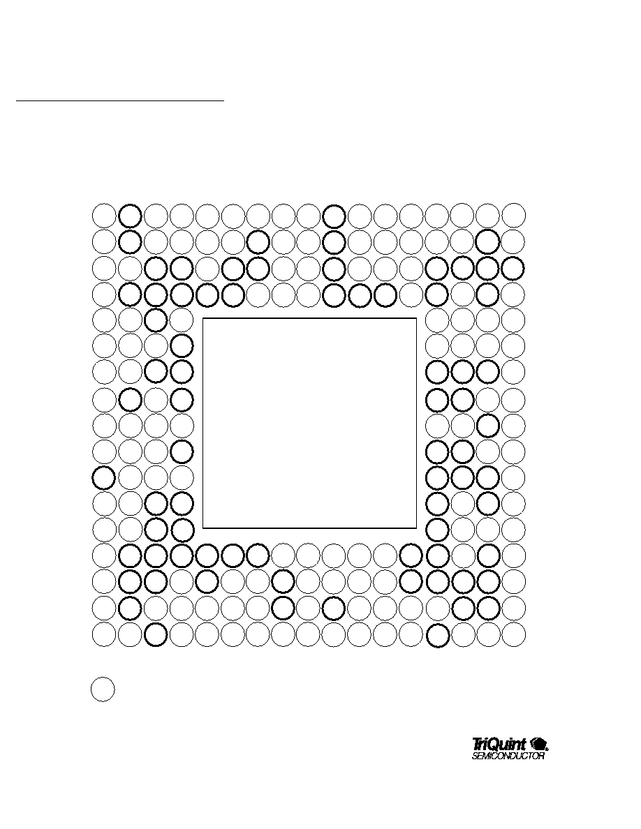
Figure 3. TQ8213 Pinout -Top View
Note: Heat Spreader is at VDD volts.
TQ8213

TQ8213
7
SONET/SDH/A
TM
PRODUCTS
PRELIMINARY DATA SHEET
TELECOM
PRODUCTS
Pin No.
Grid Ref. Signal
Type and Freq. or Bit Rate
Description
Data Multiplexing Configuration
17
A14
MODE(0) TTL
MODE(1) = N.C., MODE(0) = N.C. = 8:1 multiplexing
16
A15
MODE(1) TTL
MODE(1) = N.C., MODE(0) = VEE = 16:1 multiplexing
MODE(1) = VEE, MODE(0) = N.C. = 32:1 multiplexing
155.52 MHz, 77.76 MHz
141
P11
TD1(0)
Input TTL
Byte #1, Most significant byte. Byte wide 155.52 MHz,
155.52 MHz, 77.76 MHz
or 77.76 MHz input data. TD1(0) is the MSb
140
R11
TD1(1)
Input TTL
Mux input data bit.
139
T11
TD1(2)
Input TTL
Mux input data bit.
138
U11
TD1(3)
Input TTL
Mux input data bit.
134
U10
TD1(4)
Input TTL
Mux input data bit.
132
T9
TD1(5)
Input TTL
Mux input data bit.
135
R10
TD1(6)
Input TTL
Mux input data bit.
136
P10
TD1(7)
Input TTL
Byte 1 Mux input data bit. TD1(7) is the least significant bit.
131
P9
TDPAR1
Input TTL
Parity bit signal for the byte wide data at TD1(0) to TD1(7).
The parity bit is defined to be in parallel with the byte wide
data at TD1(0) to TD1(7) from which it was calculated.
125
U7
TD2(0)
Input TTL
Byte #2
155.52 MHz or 77.76 MHz
Byte wide 155.52 MHz or 77.76 MHz Mux input data. TD2(0)
is the most significant bit.
124
T7
TD2(1)
Input TTL
Mux input data bit.
123
U6
TD2(2)
Input TTL
Mux input data bit.
122
R7
TD2(3)
Input TTL
Mux input data bit.
119
U5
TD2(4)
Input TTL
Mux input data bit.
118
R6
TD2(5)
Input TTL
Mux input data bit.
117
T5
TD2(6)
Input TTL
Mux input data bit.
116
U4
TD2(7)
Input TTL
Byte 2 Mux input data bit. TD2(7) is LSb
130
R9
TDPAR2
Input TTL
Parity bit signal for the byte wide data at TD2(0) to TD2(7).
The parity bit is defined to be in parallel with the byte wide
data at TD2(0) to TD2(7) from which it was calculated.
77.76 MHz Interface
90
L2
TD3(0)
Input TTL 77.76Mb/s
Byte #3
Byte wide 77.76Mb/s input data. TD3(0) is the MSb.
89
P1
TD3(1)
Input TTL
Mux input data bit.
88
N1
TD3(2)
Input TTL
Mux input data bit.
87
M1
TD3(3)
Input TTL
Mux input data bit.
84
K3
TD3(4)
Input TTL
Mux input data bit.
83
K2
TD3(5)
Input TTL
Mux input data bit.
82
K1
TD3(6)
Input TTL
Mux input data bit.
81
J3
TD3(7)
Input TTL
Byte 3 Mux input data bit. TD3(7) is the least significant bit.
Table 1. Signal Description

8
TQ8213
PRELIMINARY DATA SHEET
Pin No.
Grid Ref. Signal
Type and Freq. or Bit Rate
Description
79
J2
TDPAR3
TTL
Parity bit signal for the byte wide data at TD3(0) to TD3(7).
The parity bit is defined to be in parallel with the byte wide
data at TD3(0) to TD3(7) from which it was calculated.
73
G1
TD4(0)
Input TTL 77.76Mb/s
Byte #4
Byte wide 77.76Mb/s input data. TD4(0) is the most
significant bit.
72
G2
TD4(1)
Input TTL
Mux input data bit.
71
F1
TD4(2)
Input TTL
Mux input data bit.
70
F2
TD4(3)
Input TTL
Mux input data bit.
67
E1
TD4(4)
Input TTL
Mux input data bit.
66
E2
TD4(5)
Input TTL
Mux input data bit.
65
F3
TD4(6)
Input TTL
Mux input data bit.
64
D1
TD4(7)
Input TTL
Byte 4 Mux input data bit. TD4(7) is the least significant bit.
78
J1
TDPAR4
Input TTL
Parity bit signal for the byte wide data at TD4(0) to TD4(7).
The parity bit is defined to be in parallel with the byte wide
data at TD4(0) to TD4(7) from which it was calculated.
170
P17
CK311
Output PECL 311.04 MHz
311.04 MHz clock output. Must be externally terminated by
R
Te
to V
TTe
.
171
N17
NCK311
Output PECL 311.04MHz
Complement of CK311. Must be externally terminated by
R
Te
to V
TTe
.
169
N16
CK155
Output PECL 155.52 MHz
155.52 MHz clock output. Must be externally terminated by
R
Te
to V
TTe
.
168
M15
CK78
Output TTL 77.76 MHz
77.76 MHz clock output.
167
N15
CK39
Output PECL 38.88 MHz
38.88 MHz clock output. Must be externally terminated by
R
Te
to V
TTe
.
201
E17
TDPERR
Output TTL 38.88 MHz
Parity alarm flag. Active low TTL logic signal indicating the
detection of a parity error. Remains low for at least 25 ns
when active.
200
E15
PARALM Ouput PECL 38.88 MHz
Parity alarm flag. Active high PECL logic signal indicating the
detection of a parity error. Remains high for at least 25 ns
when active. Must be externally terminated by R
Te
to V
TTe
.
2.5Gb/s Output Interface
29
A9
DOUT
Output AC 2.48832 Gb/s
High speed differential data output. DOUT is true output.
Must be AC coupled.
30
A8
NDOUT
Output AC 2.48832Gb/s
Complement of DOUT. Must be AC coupled.
22
B11
VSYMX
Input Analog DC
Rise/fall time symmetry adjust control signal input. Input
(Note 2)
impedance is typically 10 k
.
38
D7
VLEVEL
Input Analog DC
Output data amplitude adjustment control signal input. Input
(Note 2)
impedance is typically 10 k
.
26,27,28 B9,C9,D9 VDRIVE
Power rail DC
Power supply input for high power output stage, nominally at
31,32,33 B8,C8,D8
(VDD+3.3 V) or VDD.
Table 1. Signal Description (continued)

TQ8213
9
SONET/SDH/A
TM
PRODUCTS
PRELIMINARY DATA SHEET
TELECOM
PRODUCTS
Pin No.
Grid Ref. Signal
Type and Freq. or Bit Rate
Description
34
A7
VSEN1
Output Analog DC
Output current level sensing pin. VSEN1 voltage is directly
proportional to the output current level at DOUT and NDOUT.
37
A6
VSEN10
I/O Analog DC
Output current level reference pin. When driven with an
external current source at exactly 1/10 the output current
level on DOUT and NDOUT, the voltage at VSEN10 is the
equal to VSEN1.
Phase-Locked Loop Elements
182
J14
VOSC
Power rail DC
Power supply for the internal VCO.
VDD = VCO ON; VEE = VCO OFF
181
K17
VTUNEIN Input Analog
Frequency tuning voltage for the internal VCO. Negative tune
slope. Must be tied to VEE when using an external VCO.
50
A3
CLKIN
Input AC 2.48832 GHz
High frequency clock input. Must be AC coupled. The signal
must be externally terminated by R
Te
to V
TTe
. The clock
reference level is derived from V
TTe
. Must be externally
terminated by 10k
to VEE when internal VCO is used.
49
B3
NCLKIN
Input AC 2.48832 GHz
Complement of CLKIN
176
M17
HCKOUT
Output AC 2.48832 GHz
High speed clock monitor tap. 60mVpp with a 50
. load.
199
F17
CLKSEL
TTL
Clock select signal for choosing between external or internal
clock source as the active clock.
NC = External Clock Source; VEE = Internal VCO
164
T17
REFCLK
Input PECL
Reference clock input to internal phase/frequency detector.
Reference Clock
Values at REFSEL(0:2) must correspond to the reference
clock frequency being used. This signal must be externally
terminated by R
Te
to V
TTe
. When not in use tie to V
TTe.
165
R17
REFCLKT Input TTL
Reference clock input to internal phase/frequency detector.
Reference Clock
Values at REFSEL(0:2) must correspond to the reference
clock frequency being used. When not in use tie to VEE.
Reference Clock Frequency Select
196
F15
REFSEL0 TTL
(REFSEL0 = REFSEL1 = REFSEL2 = VEE)
19.44 MHz
197
F14
REFSEL1 TTL
(REFSEL0 = VDD, REFSEL1 = REFSEL2 = VEE) 38.88 MHz
198
E16
REFSEL2 TTL
(REFSEL0 = REFSEL2 = VEE, REFSEL1 = VDD) 51.84 MHz
(REFSEL0 = REFSEL1 = VDD, REFSEL2 = VEE) 77.76 MHz
(REFSEL0=VDD,REFSEL1=VEE,REFSEL2=VDD) 155.02MHz
(REFSEL0 = VEE, REFSEL1 = REFSEL2 = VDD) 311.04 MHz
(REFSEL0 = REFSEL1 = REFSEL2 = VDD) 622.08 MHz
180
L17
VTUNEO
Output Analog
Internal PLL charge pump loop filter output. Connection for
external components for the internal PLL charge pump loop
filter and to VCO tune input.
194
F16
LOCK
Output TTL
Internal PLL lock detector. Signal is high when PLL in lock.
Table 1. Signal Description (continued)

10
TQ8213
PRELIMINARY DATA SHEET
Pin No.
Grid Ref. Signal
Type and Freq. or Bit Rate
Description
Power Pins and Spare Pins
14
C11
RESET
Input PECL
Chip reset (active low). When not used must be tied to VDD
through R
Te
160
P15
PARSEL
Input TTL
When PARSEL=NC a byte-wise even parity check is
performed. When PARSEL=VEE a byte-wise odd parity
check is performed
159
U17
ID
Output Analog
Part level identification. Voltage at ID indicates device type.
187
H14
PLLVDD
Input DC
PLL positive supply voltage.
188
H15
PLLVEE
PLL supply return.
Signal
Description
Pin Number,Grid Reference
VDD
Positive rail supply voltage
9,D12
25,A10
24,B10
21,C10
20,D10
42,C6
48,D5
54,C3
55,D3
53,D4
62,F4
68,G4
74,H4
94,M4
103,P4
104,P3
109,P5
113,R5
114,P6
120,P7
127,R8
99,R2
158,R15
157,P14
161,N14
166,M14 172,L14
173,L15
178,K15
192,G14
191,G15
207,C15
208,C16
6,C14
47,C4
206,D14
145,U14
100,N4
86,L1
69,G3
VEE
Negative rail supply voltage
101,N3
102,P2
105,R3
106,T2
112,U3
128,T8
137,T10
150,R13
153,P13
154,R14
155,T15
156,T16
163,P16
174,M16
175,L16
193,G16
1,B16
2,C17
35,B7
36,C7
43,D6
51,A2
52,B2
60,D2
61,E3
76,H2
85,K4
93,M3
177,K14
184,J16
205,D16
15,D11
162,R16
NC
DO NOT CONNECT
3,B17
4,A16
5,D13
7,B15
8,C13
10,B14
11,B13
12,B12
13,C12
18,A13
19,A12
23,A11
40,B6
41,B5
44,C5
45,A4
46,B4
56,A1
57,E4
58,B1
59,C2
95,R1
96,M2
107,U1
108,U2
110,R4
111,T3
115,T4
185,J17
186,H17
151,U15
152,U16
189,H16
183,J15
195,G17
202,D17
203,E14
204,D15
121,T6
133,U9
142,U12
148,T13
149,T14
144,U13
39,A5
147,R12
146,P12
97,T1
92,L3
75,H3
98,N2
77,H1
91,L4
63,C1
80,J4
126,P8
129,U8
143,T12
179,K16
Notes:
1.Symbol definitions:
NC refers to a no-connect signal. Do Not Connect these pins!
ECL refers to an Emitter Coupled Logic signal
PECL refers to a Positive ECL
TTL refers to a Transistor-Transistor Logic signal
AC refers to AC coupled signal
2.
This signal is internally generated and can be overdriven externally.
Table 1. Signal Description (continued)

TQ8213
11
SONET/SDH/A
TM
PRODUCTS
PRELIMINARY DATA SHEET
TELECOM
PRODUCTS
Table 3. DC Operating Ranges
Table 2. Absolute Maximum Ratings
Parameter
Symbol
Min
Max
Unit
Supply voltage
VDD-VEE
0
7
V
Internal VCO Supply voltage
VOSC
VEE-0.5
VDD+0.5
V
Output stage supply voltage
VDRIVE
VDD-0.5
VDD+5.0
V
Inputs/Outputs
VEE-0.5
VDD+0.5
V
Tstg, Storage Temperature
-55
150
o
C
Tc, Maximum Case Operating Temperature
125
o
C
Tj, Maximum junction temperature
150
o
C
Electrostatic Discharge (100 pF, 1.5 k
)
1000
V
Notes:
1.
The internal VCO specification applies when Tc is within operating range. The internal VCO is operational down to -20
o
Signal
Symbol
Parameter
Min
Typ
Max
Units
VDD-VEE
V
DD
-V
EE
Supply voltage range
4.75
5.00
5.25
V
(Note 1)
VOSC
V
osc
Internal VCO supply
-
VDD
-
V
(Note 1)
I
osc
Supply current for internal VCO
14
mA
PLLVDD-PLLVEE
P
VDD
-P
VEE
PLL supply voltage
-
VDD
-
V
(Note 1)
I
PLL
Supply current for internal VCO
40
mA
VDRIVE
V
drive
Output stage power supply
+5.0
+10
+10.5
V
(Note 1)
I
drive
Supply current for output stage
150
mA
T
c
Case temperature measured at the case
-40
125
o
C
Notes:
1.
No special power up sequence is required.
2.
VEE at operating range.
Table 4. Power Dissipation
Low Speed Outputs
Driver Mod Current (mA)
VDD (V)
VDRIVE (V)
Typ Power (W)
Max Power (W)
Open
0
5.0
5.0
3.33
Open
0
5.25
5.25
4.06
Open
20 (Note 1)
5.0
5.0
3.51
Open
20
5.25
5.0
4.24
Open
60
5.0
6.75
3.96
Open
60
5.25
6.75
4.69
Open
75
5.0
10.5
4.62
Open
75
5.25
10.5
4.72
5.35
Fully Loaded
0
5.0
-
3.53
Notes:
1.
Using a Lucent D-372 laser with 20 mA of modulation current will generate 3 dBm of optical power.

12
TQ8213
PRELIMINARY DATA SHEET
Table 4. Recommended External Loop Filter Values
(for 500MHz/V KVCO)
REFCLK
Resistor
Capacitor
Capacitor
Frequency
Value R1
Value C1
Value C2
(MHz)
(
)
(
µ
F)
(pF)
19.44
2.2k
0.1
5.1
38.88
1.2k
0.1
8.6
51.84
910
0.1
11.2
77.76
600
0.1
17
155.52
600
0.1
17
311.04
600
0.1
17
622.08
600
0.1
17
C1
R1
VTUNEO
PLLVDD
C2
Table 6. VCO Control Signal Specifications
Signal
Symbol
Parameter
Min
Typ
Max
Units
VTUNEO
V
range
VTUNEO voltage range (Note 1)
2.5
V
KVCO
VCO VTUNE voltage gain
500
MHz/V
f
range
VCO frequency range when using internal PLL
1950 - 2700
MHz
Notes:
1. A VTUNEO voltage of 2.5V corresponds to approximatey a 2.5GHz center frequency.
Table 7. Driver Control Signal Specifications
Signal
Symbol
Parameter
Min
Typ
Max
Units
VSYMX
V
symx
VSYMX overdrive voltage linear range
V
def
-1
V
def
V
def
+1
V
A
symx
Output data crossing level adjust gain
15
%/V
V
def
Default output level (Note 1)
1.88
V
Z
symx
VSYMX input impedance
10
k
VLEVEL
V
level
VLEVEL overdrive voltage linear range
0.5
-
2.5
V
A
amp
Output data amplitude adjust gain
1.6
V/V
Z
level
VLEVEL input impedance
10
k
VSEN1
R
sen1
VSEN1 equivalent resistance
4.5
5
5.5
I
sen1
VSEN1 input current range
20
150
mA
VSEN10
R
sen10
VSEN10 equivalent resistance
45
50
55
I
sen10
VSEN10 input current range
2
15
mA

TQ8213
13
SONET/SDH/A
TM
PRODUCTS
PRELIMINARY DATA SHEET
TELECOM
PRODUCTS
Table 8. 2.5GHz and 2.5Gb/s High Speed Signal Specifications
Signal
Symbol
Description
Min
Nom
Max
Units
CLKIN
tcki
Input clock period
370.4 ps
401.88 ps 250 ns
NCKLIN
tckdc
Input clock duty cycle (Note 1)
40
50
60
%
Vpp
Input clock peak-to-peak voltage
1000
1200
1400
mV
DOUT
Tpw
Output data pulse width
95
100
105
%
NDOUT
Trise
Output data rise time
-
-
130
ps
(Note 2)
Tfall
Output data fall time
-
-
130
ps
Jpp
Output data peak-peak jitter (Note 3)
-
8
20
ps
V
mean_max
Output data mean pk-pk for high output applications;
3.75
V
Vdrive = +10 V
V
mean_min
Output data mean pk-pk for high output applications;
0.5
V
Vdrive = +5 V
X
ingmin
Min. data crossing level adjustment range with VSYMX at 1.38
30
35
40
%
X
ingmax
Max. data crossing level adjustment range with VSYMX at 2.38
60
65
70
%
DXing
Absolute variation in output data crossing level over full
-5
-
+5
%
VLEVEL operating range
%over
Overshoot
-
-
10
%
%under
Undershoot
-
-
10
%
%ripple
Ripple
-
-
10
%
HCKOUT
thcko
High speed output clock period
-
401.88
-
ps
Vpp
High speed output clock peak-to-peak voltage
10
-
-
mV
R
Te
High speed output clock output impedance
45
50
55
Notes:
1.Defined as percentage of the input clock period. Duty cycle is measured at the average voltage of the signal.
2.Refer to Figure 9. All specifications for output data apply under the following conditions:
Output Data Pattern:
2
23
-1 PRBS, 2.48832 Gbit/s
DOUT and NDOUT termination:
50
to VEE
Termination network return loss:
>20 dB, 0 to 1 GHz
>10 dB, 1 to 3 GHz
>6 dB, 3 to 5 GHz
Vlevel:
over specified operating range
VSYMX:
adjusted to give 50% data crossing
3.Specified as the peak to peak jitter shown in Figure 9. This specification does not include the reference clock and measurement
system jitter. This is accomplished by first measuring the peak-to-peak jitter of the reference clock and
subtracting this value from the measured peak-to-peak jitter for the device under test using the same measurement system.
Table 9. Jitter Transfer Performance
Symbol
Description
Nom
Max
Units
J
peaking
Peak Gain in Transfer Curve
0.02
0.1
dB
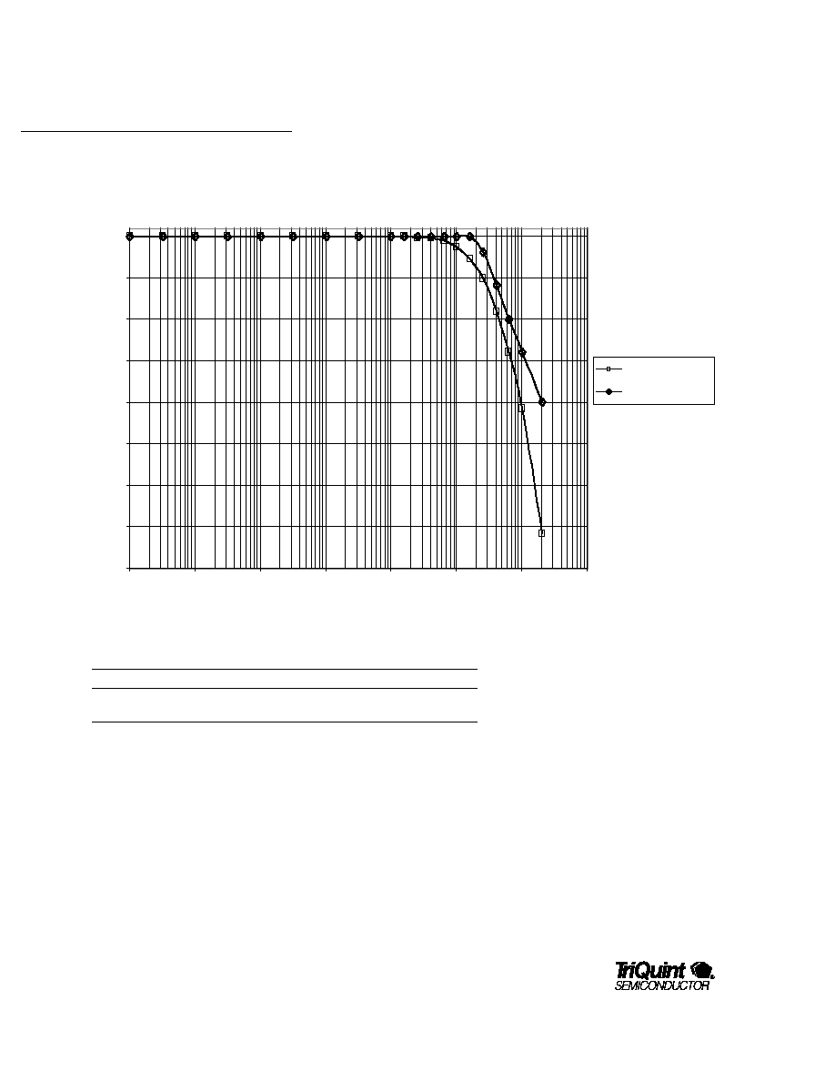
f
c
Corner Frequency Transfer Curve
1.54
2.0
MHz
Note: Jitter Transfer measurments were
performed with the PLL loop filter values
specified in Table 5. The method used is
outlined in a Jitter Bench application note
available upon request. The values listed as
nominal were performed under the following
conditions: DOUT = 3.5 Vp-p
VDD = 5 V
Tcase = 60 C

14
TQ8213
PRELIMINARY DATA SHEET
Table 10. Jitter Generation Performance
Jitter Generation
Nom
Max
Units
J
PP
6.0
20
ps
J
RMS
1.0
2.0
ps
Note: Jitter Generation measurments were performed
with the PLL loop filter values specified in Table 5.
The method used is outlined in a Jitter Bench
application note available upon request. The values
listed as nominal were performed under the following
conditions: Data Rate = 2.48832 Gb/s
DOUT = 3.5 Vp-p
VDD = 5 V
Tcase = 60 C
-40
-35
-30
-25
-20
-15
-10
-5
0
1.E+01
1.E+02
1.E+03
1.E+04
1.E+05
1.E+06
1.E+07
1.E+08
Transfer, 5.0V, 50C
SONET/SDH Template
Figure 4. Typical Jitter Transfer Curve (REFCLK = 77.76 MHz)
Gain (dB)
Frequency (Hz)

TQ8213
15
SONET/SDH/A
TM
PRODUCTS
PRELIMINARY DATA SHEET
TELECOM
PRODUCTS
Table 11. PECL Interface Specifications
Signal
Symbol
Description
Min
Nom
Max
Units
CK311
tckdc
Output clock duty cycle (Note 2)
40
50
60
%
NCK311
tckr
Output clock rise time (20% to 80%)
750
ps
CK155
tckf
Output clock fall time (20% to 80%)
750
ps
CK39
Voh
Output clock high level
V
DD
-1.0
V
DD
-0.6
V
(Note 1)
Vol
Output clock low level
V
TTe
V
DD
-1.6
V
Vamp
Output clock amplitude (Note 3)
+/-350
mV
RESET
trf
Reset fall time (20% to 80%)
300
ps
REFCLK
Vih
Input high level
V
DD
-1.05
V
DD
-0.4
V
Vil
Input low level
V
TTe
V
DD
-1.55 V
PARALM Voh
Output high level
V
DD
-1.0
V
DD
-0.6
V
Vol
Output low level
V
TTe
V
DD
-1.6
V
Notes:
1. All specifications apply with CK311 CK155 and CK39 terminated with R
Te
to V
TTe
.
2.Output clock duty cycle is measured at the mean voltage of the signal and nominal input clock frequency of 2.48832GHz.
3.The CK311, CK155 and CK39 clock output amplitude is measured with respect to the mean voltage of the signal.
Table 12. TTL Interface Specifications
Signal
Symbol
Description
Min
Nom
Max
Units
CK78
tckdc
78 MHz output clock duty cycle (Note 1)
40
50
60
%
LOCK
tckr
78 MHz output clock rise time (20% to 80%)
2000
ps
TDPERR
tckf
78 MHz output clock fall time (20% to 80%)
2000
ps
(Note 2)
Voh
Logic output high level
2.4
V
DD
V
Vol
Logic output low level
V
EE
0.4
V
Cload
Output load capacitance
20
pF
TD1(0:7)- Tsu
Input data setup time (Note 2)
500
ps
TD4(0:7) Tho
Input data hold time (Note 2)
2500
ps
TDPAR1- Vih
Input data high voltage (Note 3)
V
DD
-3.0
V
DD
V
TDPAR4
Vil
Input data low voltage (Note 3)
V
EE
V
EE
+0.8
V
Iih
Input data high-level input current
-
-
200
uA
Iil
Input data low-level input current
-400
-200
-
uA
Cin
Input data capacitance
10
pF
MODE(0:1)Vih
Logic input high level
2.0
V
DD
V
PARSEL
Vil
Logic input low level
V
EE
0.8
V
REFSEL(0:2)
REFCLKT
Notes:
1.Output clock duty cycle is measured at the mean voltage of the signal and nominal input clock frequency of 2.48832GHz.
2.The parity alarm flag TDPERR is an active LOW TTL signal. When a parity error is detected, TDPERR must remain active (logic
LOW) for the minimum duration of 25 ns The occurrence of further parity errors during this hold time when TDPERR is active will
be ignored.
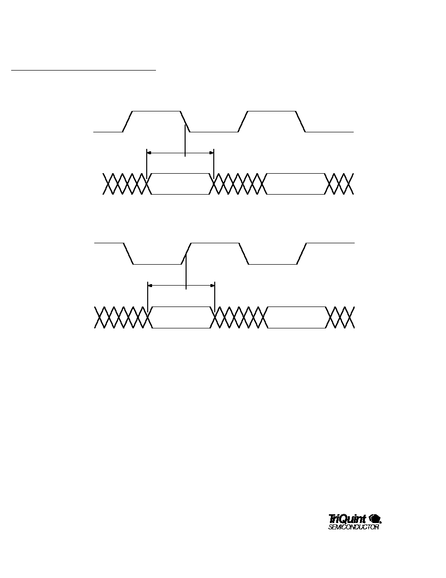
3.Tsu and Tho are specified relative to the rising edge of CK78 and the falling edge of CK155. See Figure 5 and Figure 6. Input data
edge jitter is not included in the specifications. The input data bus bits are assumed to be free of any skewing in time.
The specifications apply under the following conditions:
Input data rise/fall time:
< 800ps (20% to 80%)
Input data:
2
23
-1 PRBS, 16x155 Mb/s or 32x77.76 Mb/s
Output clock frequency:
155.52MHz or 311.04MHz
Output CK155 termination:
RTe to VTTe

16
TQ8213
PRELIMINARY DATA SHEET
CK155
TD1(0:7)
TD2(0:7)
T
su
T
ho
Valid
Data
Valid
Data
Figure 5. AC Timing: 155.52 Mb/s
CK78
TD1(0:7)
TD2(0:7)
TD3(0:7)
TD4(0:7)
T
su
T
ho
Valid
Data
Valid
Data
Figure 6. AC Timing: 77.76 Mb/s

TQ8213
17
SONET/SDH/A
TM
PRODUCTS
PRELIMINARY DATA SHEET
TELECOM
PRODUCTS
Table 13. Output Clock Timing Relationships
Symbol
Description
Typ
Max
Units
T
CK155
CK311 to CK155 timing relation
502
pS
T
CK78
CK311 to CK78 timing relation
78
pS
T
CK39
CK311 to CK39 timing relation
1800
pS
Figure 7. Output Clock Timing Relationships
CK311
CK155
CK78
CK39
T
CK155
T
CK78
T
CK39
Table 14. Reference and Bus Clock Timing Relationship
REFCLK
Bus Clock
Symbol
Description
Min
Typ
Max
Units
77.76 MHz TTL
CK78
T
SKEW
Falling Edge Time Offset
10.2
11.2
12.5
nS
77.76 MHz PECL
CK78
T
SKEW
Falling Edge Time Offset
10.1
11.1
12.3
nS
155.52 MHz TTL
CK155
T
SKEW
Falling Edge Time Offset
5.0
5.7
6.7
nS
155.52 MHz PECL
CK155
T
SKEW
Falling Edge Time Offset
4.9
5.6
6.5
nS
Figure 8. Reference and Bus Clock Timing Relationship
REFCLK
Bus Clock
T
SKEW

18
TQ8213
PRELIMINARY DATA SHEET
Mean `1' Level
T
rise
, T
fall
Mean `0' Level
V
ripple
J
pp
T
pw
V
over
V
under
100%
80%
20%
0%
Data
Crossing
Meas.
T
rise
, T
fall
V
ripple
J
pp
V
mean
V
min
V
max
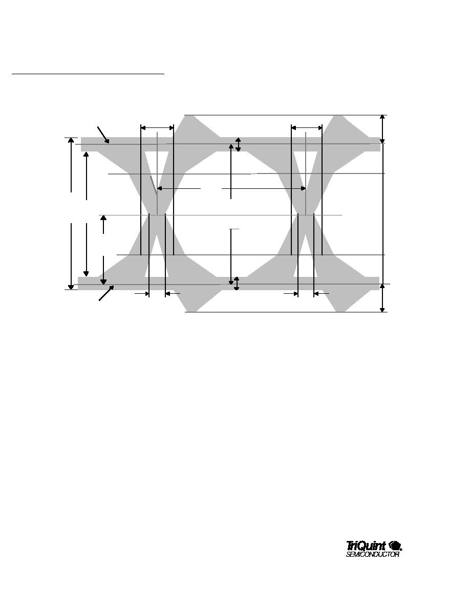
Figure 9. 2.5 Gb/s Output Data Eye Diagram
T
pw
=
half of input waveform period
V
max
=
maximum peak-to-peak voltage
V
min
=
minimum peak-to-peak voltage (eye interior)
V
mean
=
Mean peak-to-peak voltage (mean eye opening)
T
rise
=
20% to 80% rise time, mean `0' to mean `1'
T
fall
=
20% to 80% fall time, mean `0' to mean `1'
%
over
=
Vover/Vmean X 100%
%
under
=
Vunder/Vmean X 100%
%
ripple
=
Vripple/Vmean X 100%
J
pp
=
peak-to-peak data crossing jitter
Note: mimimum display persistence of 2 s is assmed for the above
measurements.

TQ8213
19
SONET/SDH/A
TM
PRODUCTS
PRELIMINARY DATA SHEET
TELECOM
PRODUCTS
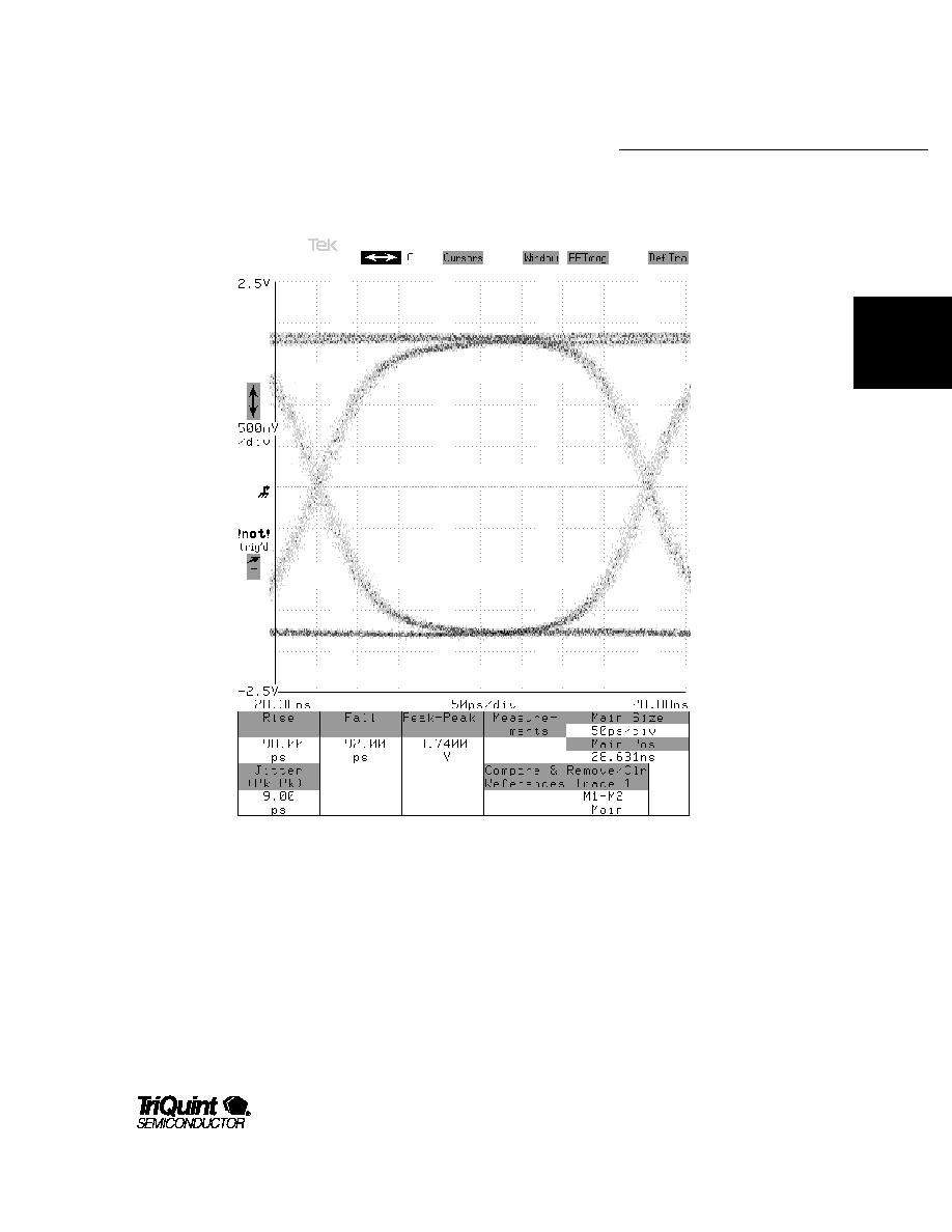
Figure 10. Typical 2.5 Gb/s Output Data Eye Scope Shot

20
TQ8213
PRELIMINARY DATA SHEET
V
e
VDD
GND
VEE (GND)
N.C.
2.5GHz clock monitor
38.88MHz
A.C.
Terminated
Variable
Current
Source
2.48832Gb/s
+5.0V
VEE (GND)
+8.3V
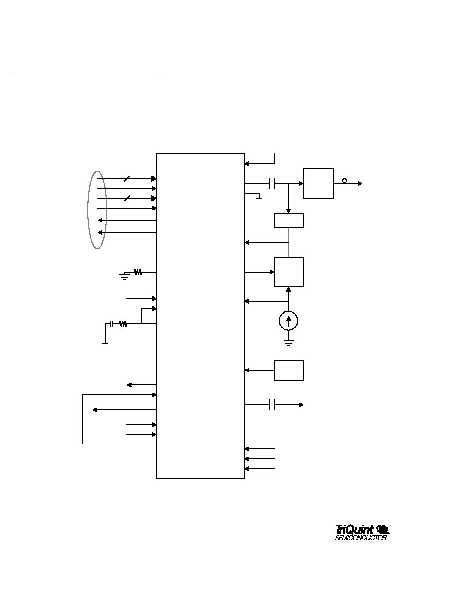
Figure 8. TTL 16:1 Multiplexing Application with Internal PLL and VCO
VSYMX
Control
VLEVEL
VTUNEIN
CLKIN
CLKSEL
VDRIVE
VSEN1
DOUT
VTUNEO
VSEN10
LOCK
CK155
CK39
HCKOUT
NDOUT
MODE(0)
MODE(1)
VSYMX
TDPERR
TD1(0)-TD1(7)
VOSC
TDPAR1
REFCLK
TDPAR2
TD2(0)-TD2(7)
VEE
VDD
E/O
Module
Peak
Detector
System
38.88Mhz
155.53Mb/s TTL Inter
face
Typical Application

TQ8213
21
SONET/SDH/A
TM
PRODUCTS
PRELIMINARY DATA SHEET
TELECOM
PRODUCTS
V
e
e
+5.0V
GND
N.C.
VEE (GND)
2.5GHz clock monitor
38.88MHz
A.C.
Terminated
Variable
Current
Source
2.48832Gb/s
VEE (GND)
VDD
+8.3V
VSYMX
Control
VLEVEL
VTUNEIN
CLKIN
CLKSEL
VDRIVE
VSEN1
DOUT
VSEN10
CK78
CK39
HCKOUT
NDOUT
MODE(0)
MODE(1)
VSYMX
BRV
TDPERR
TD10-TD17
VOSC
TDPAR1
TDPAR4
TDPAR2
TDPAR3
TD40-TD47
TD30-TD37
TD20-TD27
VEE
VDD
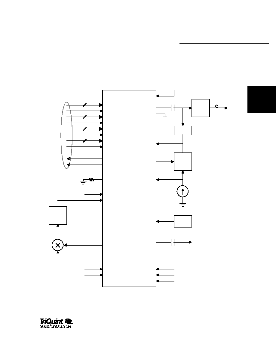
Figure 9. 32:1 Multiplexing Application with External PLL and Internal VCO
E/O
Module
Peak
Detector
System
38.88Mhz
77.76Mb/s TTL Interface

22
TQ8213
PRELIMINARY DATA SHEET
Symbol
Parameter
Min
Nom
Max
A
Overall Thickness
1.45
1.55
1.65
A1
Ball Height
0.60
0.65
0.70
D
Body Size
22.80
23.00
23.20
D1
Ball Footprint
20.32 (BSC.)
E
Body Size
22.80
23.00
23.20
E1
Ball Footprint
20.32 (BSC.)
b
Ball Diameter
0.65
0.75
0.85
c
Body Thickness
0.85
0.90
0.95
aaa
Seating Plane Clearance
0.15
e
Ball Pitch
1.27 TYP.
P
Encapsulation Clearance
0.15
Top view
Bottom view
Side View Section
D
E
A1 Ball I.D. Mark
45
o
0.5mm Chamfer
A
B
C
D
E
F
G
H
J
K
L
M
N
P
R
T
U
17 16 15 14 13 12 11 10 9 8 7 6 5 4 3 2 1
D1
E1
e
e
b
A1 Ball
Corner
A
A1
C
aaa
P
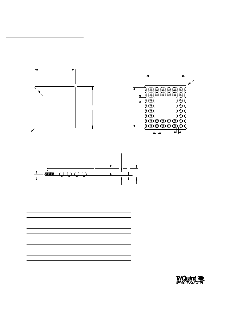
Figrure 10. 208-pin BGA Mechanical Dimensions
Table 9. 208-pin BGA Dimensions
Note: Heat Spreader is at VDD volts.
Note: All dimensions in millimeters (mm)

TQ8213
23
SONET/SDH/A
TM
PRODUCTS
PRELIMINARY DATA SHEET
TELECOM
PRODUCTS
The information provided herein is believed to be reliable; TriQuint assumes no liability for inaccuracies or
omissions. TriQuint assumes no responsibility for the use of this information, and all such information
shall be entirely at the user's own risk. Prices and specifications are subject to change without notice.
No patent rights or licenses to any of the circuits described herein are implied or granted to any third party.
TriQuint does not authorize or warrant any TriQuint product for use in life-support devices and/or systems.
www.TriQuint.com
Copyright © 1999 TriQuint Semiconductor, Inc. All rights reserved.
Revision 0.3.A June 1999

