 | –≠–ª–µ–∫—Ç—Ä–æ–Ω–Ω—ã–π –∫–æ–º–ø–æ–Ω–µ–Ω—Ç: TQ8223CDR | –°–∫–∞—á–∞—Ç—å:  PDF PDF  ZIP ZIP |

T
R
I Q
U
I
N
T
S E M I C O N D U C T O R , I N C .
PRELIMINARY DATA SHEET
TELECOM
PRODUCTS
1
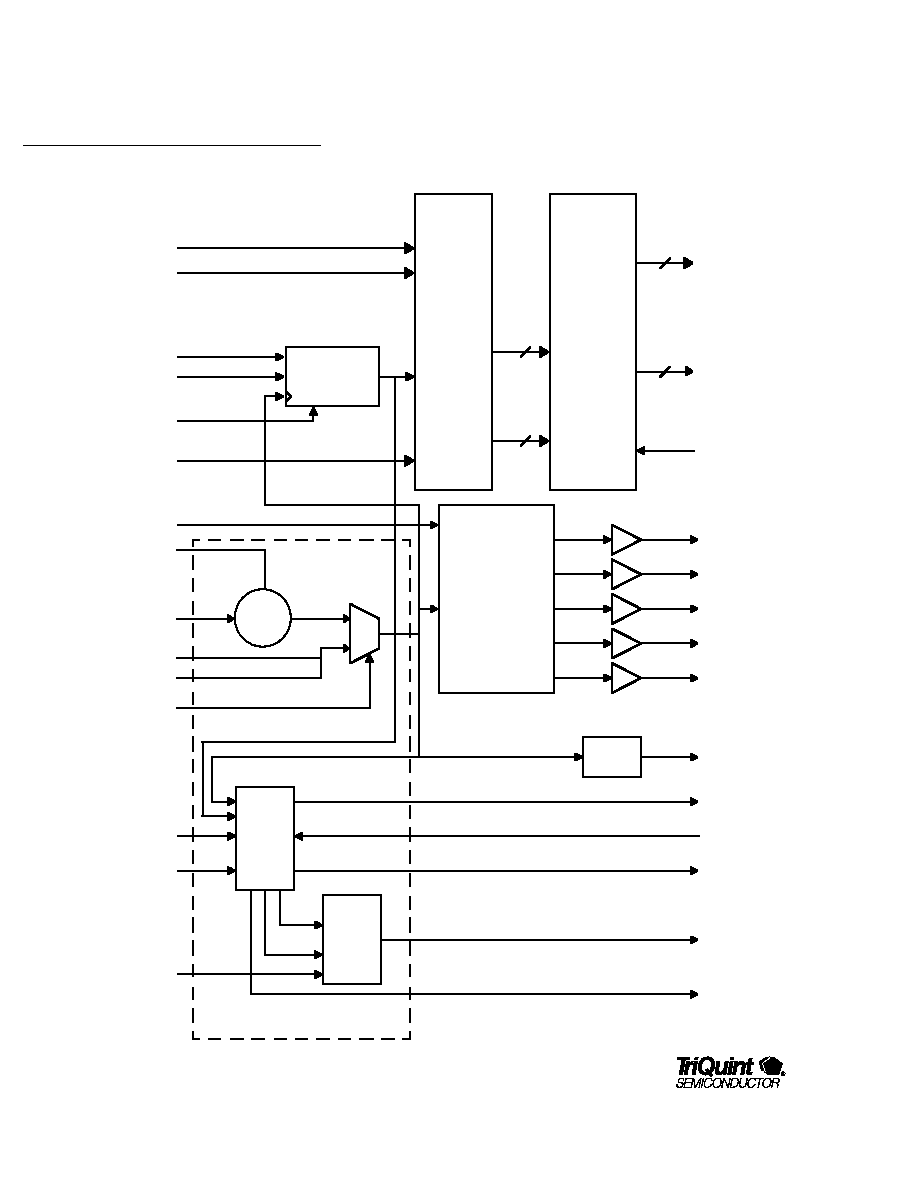
The TQ8223 is a multi-configuration SONET/SDH OC48/STM16 CDR/
DEMUX that regenerates and re-times serial 2.48832 Gb/s data. It
recovers the 2.48832 GHz clock from the data stream and frequency
divides it to generate control signals and clocks used to perform the
demultiplexing function.
The TQ8223 is extremely flexible for telecom, ATM and networking
applications. The serial 2.48832 Gb/s data stream is demultiplexed into a
32-bit wide 77.76 MHz TTL data bus. Internal data inversion is also
available. The device generates byte-wise parity check bits for the
demultiplexed data and provides associated clock outputs for the different
modes. Parity checking is not required for normal device operation.
The TQ8223 provides added flexibility through a selectable internal/external
Voltage Controlled Oscillator(VCO) as well as a selectable internal Phase
Locked Loop (PLL). If an external high frequency clock is utilized a single-
ended or differential AC coupled clock may be used.
The internal PLL contains a NRZ phase detector which enables it to adjust
the phase of the internal clock such that sampling of the incoming data
stream occurs in the middle of the the data eye. An offset control allows
adjustment
±
125 pS around this nominal position.
Operating from a single +5V supply, the TQ8223 provides fully compliant
functionality and performance.
The TQ8223 is fully compliant with SONET/SDH jitter tolerance and
transfer specifications. A TTL level LOCK signal is supplied to indicate
when the frequency difference between the internal 38.88 MHz clock and
the external 38.88 MHz clock is less than 488 ppm.
OC48/STM16
DEMUX/CDR
with Differential Input
Features
∑ Single-chip 1:32 Demultiplexer
with integrated clock and data
recovery
∑ Differential Analog Data Input
∑ SONET/SDH compliant for
2.48832 Gb/s jitter tolerance &
transfer
∑ Internal PLL with NRZ phase
detector ensures sampling of
incoming data stream occurs in
center of data eye
∑ Static phase adjustment on
recovered clock position
∑ High speed input data bit slipper
for use in framing
∑ External RC-based loop filter
∑ Four output clock rates at
311.04, 155.52, 77.76, and 38.88
MHz.
∑ Internal byte-wise even/odd
parity bit generator (mode
programable)
∑ Direct-coupled TTL low-speed
outputs
∑ 23mm 208-pin BGA package
∑ 5V single supply
∑ ≠40 to +125
∞
C case operating
temperature.
TQ8223

2
TQ8223
PRELIMINARY DATA SHEET
LOCKREF
LOCK
CK311
CK155
CK78T
NCK311
Figure 1. TQ8223 Block Diagram
VTUNEO
CK39
HCKOUT
DIN
VOSC
VTUNE
CLKIN
CLKSEL
DCREF
MODE0
MODE1
PHADJ
DATINV
PHREF
RQ1n-RQ4n
RQPAR1-4
HINTCLK
PPMSEL
NCLKIN
PARSEL
SLIP
RESET/RSTN
NDIN
DEMUX
Parity
Generator
and
Output
Register
Internal PLL
NRZ
Phase
Detector
and
LOCK
Detect
Data
Regenerator
VCO
50
Resistive
Tap
2.48832GHz
Clock Input
Selector
Active Clock
32
1
0
Clock Divider
4
Charge
Pump

TQ8223
3
SONET/SDH/A
TM
PRODUCTS
PRELIMINARY DATA SHEET
TELECOM
PRODUCTS
Function Description
Data Regeneration
The TQ8223 recovers and regenerates serial 2.48832
Gb/s data received at DIN and NDIN. The data recovery
can be optimized by adjusting the input data re-timing
clock phase at PHADJ. The PHADJ range is 2.5 +/-
0.5V. This corresponds to a centered sampling point
when PHADJ is 2.5V and a -128 pS or +128 pS offset
for 3V and 2V repectively. PHADJ must be externally
supplied. See the figure below.
The regenerated data is then re-synchronized by re-
timing it with the active 2.48832 GHz clock. (Negative
edge triggered sampling is used.)
The regenerated data can be inverted by tying the
DATINV pin to VEE.
Bit Slipper
The TQ8223 can slip a bit on the incoming data stream.
An active low PECL pin, SLIP, causes the TQ8223 to
skip over one incoming data bit. This can be done for
framing purposes.
Timing Generation
The TQ8223 can receive an external 2.48832 GHz
(nominal) reference clock or generate a 2.48832 GHz
clock through an internal VCO. The output of the active
clock can be monitored at HKCOUT which provides a
30mV
pp
output.
Internal Clock VCO and PLL
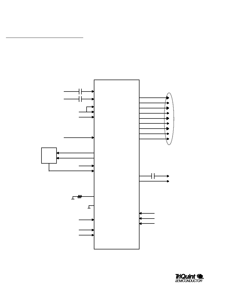
Figure 8 contains a reference diagram of operation with
the internal clock and PLL. The internal clock is
selected if the CLKSEL is tied to VDD and the external
LOCK Signal Hysteresis
Clock Freq. Difference
LOCK
HIGH
LOW
488ppm
30ppm
or
122ppm
2.5V
0pS
2.0V
128pS
3.0V
-128pS
Time
PHADJ
PHADJ Operation
power supply pin, VOSC, is tied to VDD. CLKIN must be
tied to VEE through a 10k
resistor when the internal
clock is used.
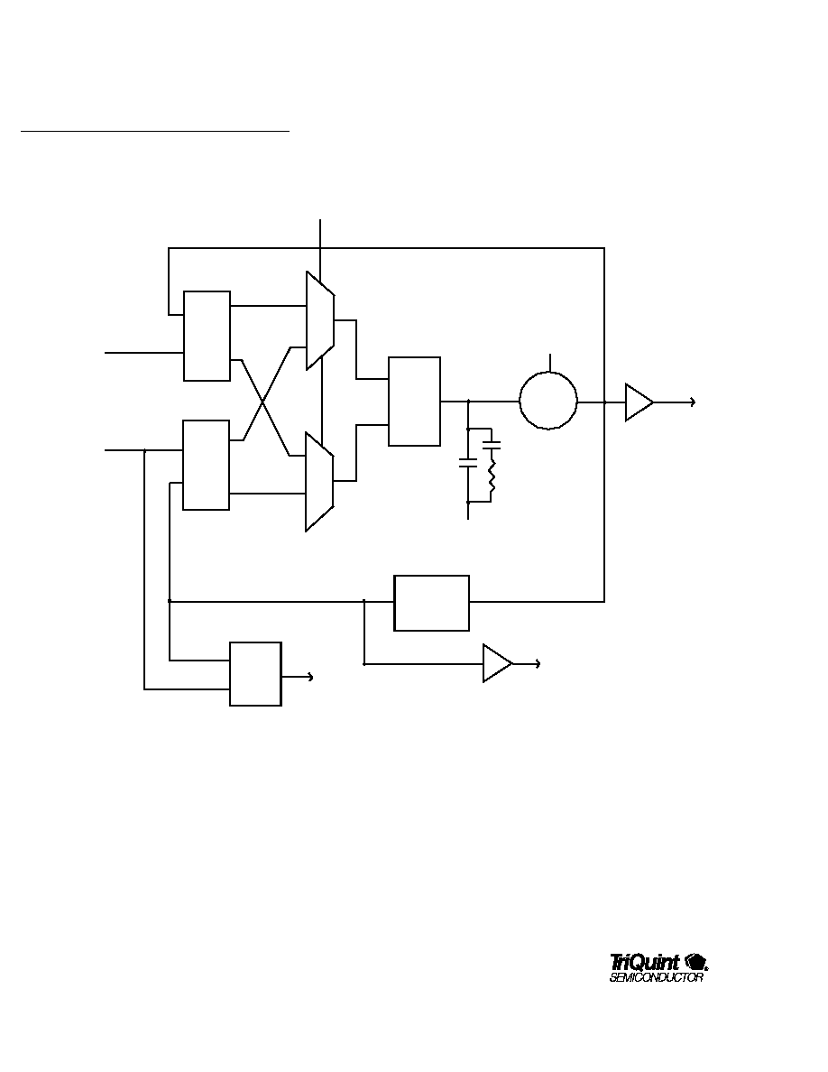
The internal PLL is comprised of a NRZ phase detector,
a charge pump, and the internal VCO. This NRZ phase
detector's phase error signals are integrated by the
Charge Pump block which then provides a VCO tune
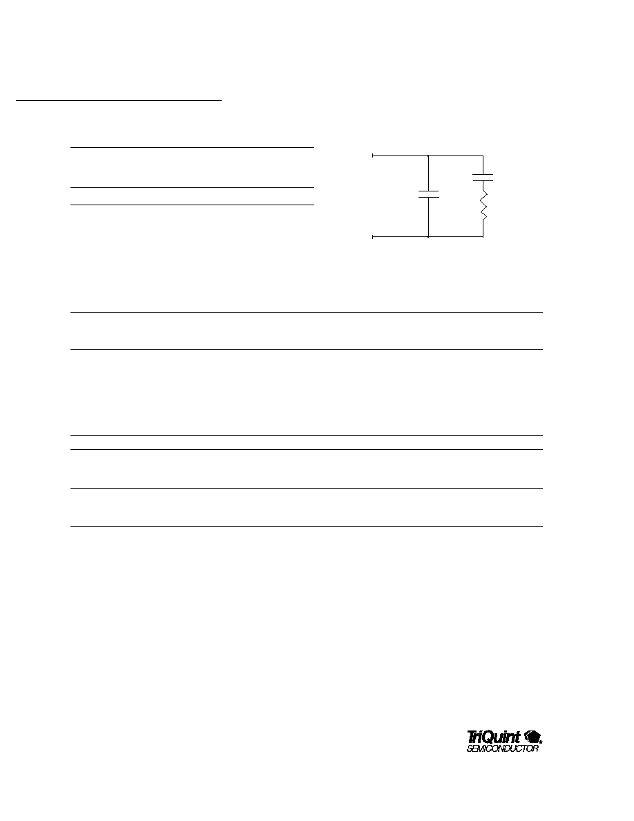
voltage at VTUNEO. See Table 5 for loop filter values.
The internal PLL is completed by connecting VTUNEO
to VTUNE. The purpose of the internal PLL is to adjust
the phase of the internal VCO such that the negative
edge of the internal sampling clock is in the center of
the data eye. A phase offset can be added by adjusting
the PHADJ input voltage. A 38.88 MHz PECL clock
must be provided at HINTCLK to aid PLL acquisition.
The internal PLL provides an active high LOCK signal if
the frequency difference between the internal VCO and
the 38.88 MHz hint clock remains less than 488 ppm. If
the frequency difference becomes greater than 488
ppm then the LOCK signal deasserts low. The LOCK
signal will assert high when the frequency difference is
less then 122 ppm or 30 ppm. This hysteresis set point
is programmable and is determined by PPMSEL. When
PPMSEL is tied to VEE the LOCK set point is 30 ppm,
when PPMSEL is tied to VDD the LOCK set point is 122
ppm.

4
TQ8223
PRELIMINARY DATA SHEET
External Clock VCO and PLL
The received clock can be either single-ended or
differential and is an AC coupled input on CKIN and
NCKIN. The external clock is selected as the active
clock if CLKSEL is tied to VEE. VOSC and VTUNE must
be tied to VEE when using an external VCO. If the
external clock is single ended the unused input must be
externally terminated through a capacitor to an AC
ground. The internal NRZ phase detector generates
Figure 2. PLL and Lock Detector Block Diagram
PLLVDD
VTUNE
VTUNEO
VCO
VOSC
HCKOUT
CLOCK
DIVIDER
LOCK
DETECT
CK38
HINTCLK
(N)DIN
Up
Up
Dn
Dn
LOCK
UP
DOWN
CHARGE
PUMP
PHASE
DETECT
PHASE
FREQ
DETECT
LOCKREF
2 : 1
2 : 1
PHREF and DCREF which, when connected to an
external integrator, may be used to tune the external
VCO.

TQ8223
5
SONET/SDH/A
TM
PRODUCTS
PRELIMINARY DATA SHEET
TELECOM
PRODUCTS
Internal Clock VCO and External PLL
See Figure 9 for a reference diagram of operation with
the internal clock and external PLL. PHREF and DCREF
must be connected to an external integrator. The output
of the integrator is then connected to VTUNE,
completing the PLL.
Output Clocks
The TQ8223 provides an internal Clock Divider which
frequency divides the active 2.48832 GHz clock
(internal or external source as selected by CLKSEL).
The output of the Clock Divider supplies the internal
clock signals necessary for the re-timing function and
demultiplexing function. Clock Divider block also
outputs four external clocks: a differential 311.04 MHz
PECL clock at CK311 and NCK311, a 155.52MHz PECL
clock at CK155, a 77.76 MHz TTL clock at CK78T, and a
38.88 MHz PECL clock at CK39. Note that the clock
frequencies given above are dependant upon using the
part at 2.48832 GHz.
Data Demultiplexer and Parity Generator
The TQ8223 can be configured to run in one of two
modes. The demultiplexing modes are set by fixing the
MODE1 and MODE0 package pins according to the
following table.
MODE1
MODE0
Demultiplexing Mode
VEE
N.C.
1:32
VEE
VEE
ALL 1's OUTPUTS
For all modes the first high speed input bit in time
appears on RQ11, which is the most significant bit.
Subsequent input data is output sequentially to RQ12-
RQ48. Byte #1, RQ11-RQ18, is the most significant
byte. Odd or even parity selection is programmable by
PARSEL. If PARSEL is left open (N.C.) the parity is
even. If PARSEL is tied to VEE the parity is odd.
In a 1:32 demultiplexing application, the TQ8223
regenerates the serial 2.48832 Gb/s data stream and
re-times it with the negative edge of the active 2.48832
GHz clock. The re-timed serial data stream is then 1:32
demultiplexed by the DEMUX block into an 32-bit wide
77.76 MHz data bus at RQ11-RQ48. A parity bit is
generated for each byte, and transmitted in parallel to
the data at RQPAR(1:4). The 32-bit wide data plus four
parity bits are then clocked out on the falling edge of
the internally generated 77.76 MHz clock. See Figure 6.

6
TQ8223
PRELIMINARY DATA SHEET
208-pin BGA
Top View
17
11
10
9
16
15
14
13
12
8
7
6
5
4
3
2
1
A
B
C
D
E
F
G
H
J
K
L
M
N
P
R
T
U
NC
(Do Not Connect)
=
RQ12
RQ13
RQ14
RQ18
RQ17
RQ16
RQ15
RQPAR1
NCK311
CK311
DIN
NDIN
PPMSEL
17
11
10
9
16
15
14
13
12
8
7
6
5
4
3
2
1
A
B
C
D
E
F
G
H
J
K
L
M
N
P
R
T
U
RQ28
RQ24
RQ22
RQ21
RQ23
RQ27
RQ26
RQ25
RQPAR2
RQ31
RQ32
RQ33
RQ34
RQ35
RQ36
RQ37
RQ38
RQPAR3
RQ41
RQ42
RQ43
RQ44
RQ45
RQ46
RQ47
RQ48
RQPAR4
CK155
CK78T
SLIP
PHREF
VDT1
VDT1
VDT1
VDT2
VDT2
VDT2
VOSC
VTUNE
MODE0
MODE1
CK39
HCKOUT
CLKSEL
HINTCLK
PARSEL
TB_UPDN
TESTMODE
VTUNEO
LOCK
RESET
ID
PLLVDD
PLLVEE
DATINV
RQ11
CKIN
NCKIN
DCREF
PHADJ
LOCKREF
RSTN
CVDD
CVDD
VDD
VDD
VDD
VDD
VDD
VDD
VDD
IOVDD
VDD
VDD
VDD
VDD
IOVDD
VDD
VDD
VDD
VDD
VDD
VDD
VDD
VDD
IOVDD
VDD
VDD
VDD
VDD
VEE
VEE
VEE
CVEE
IOVEE
IOVEE
VEE
IOVEE
VEE
IOVEE
IOVEE
IOVEE
VEE
VEE
VEE
VEE
VEE
VEE
IOVEE
VEE
IOVEE
VEE
VEE
VEE
VEE
VEE
IOVEE
VEE
VEE
IOVEE
VEE
VEE
VEE
IOVDD
IOVDD
IOVDD
IOVDD
IOVDD
IOVDD
IOVDD
IOVDD
IOVDD
IOVDD
IOVDD
IOVDD
IOVDD
IOVDD
IOVDD
IOVDD
IOVDD
IOVDD
CVEE
IOVEE
VEE
TQ8223
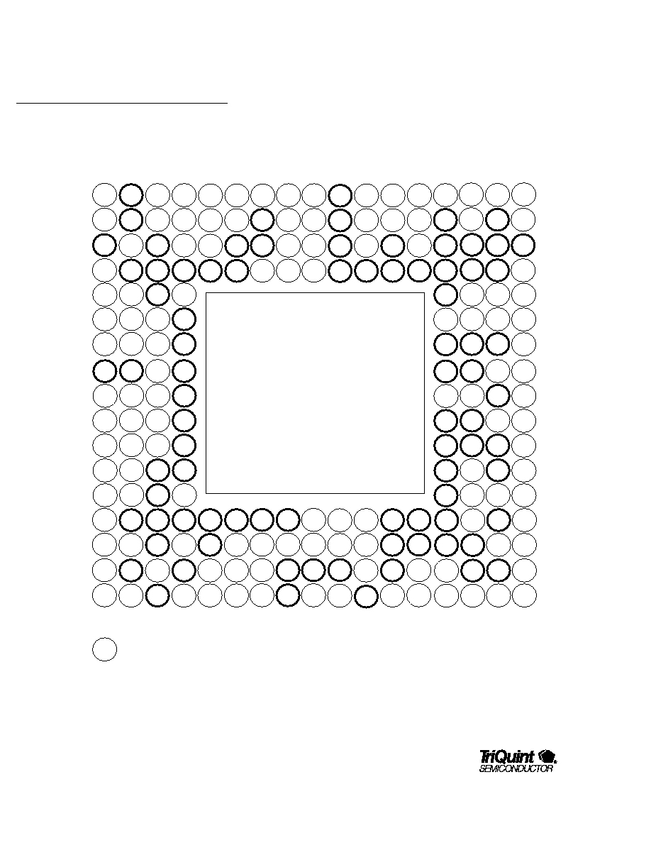
Figure 3. TQ8223 Pinout - Top View
Note: Heat Spreader is at VDD volts.

TQ8223
7
SONET/SDH/A
TM
PRODUCTS
PRELIMINARY DATA SHEET
TELECOM
PRODUCTS
Table 1. Signal Description
Pin No.
Grid Ref. Signal
Type & Freq/Bit Rate Description
Data Demultiplexing Configuration
50
A3
MODE0
Input DC
(MODE1 = N.C., MODE0 = N.C.) = Do Not Use;
49
B3
MODE1
Input DC
(MODE1 = N.C., MODE0 = VEE) = 1:16 demultiplexing;
(MODE1 = VEE, MODE0 = N.C.) = 1:32 demultiplexing;
(MODE1 = VEE, MODE0 = VEE) = all 1's output.
2.5Gb/s Input Interface
30
A8
DIN
Input AC 2.48832 Gb/s
High speed differential data input. Must be AC coupled.
29
A9
NDIN
The input is internally terminated by R
T
to V
TD1,2
.
26,27,28 B9,C9,D9 VTD2
Input Analog DC
Input signal termination voltage, nominally at V
DD
-2.8V.
31,32,33 B8,C8,D8 VTD1
Input Analog DC
46
B4
DATINV
Input Analog DC
DIN complement select signal.
N.C. = true; VEE =complement
77.76Mb/s Interface
142
U12
RQ11
Output TTL
Byte #1. Most significant Byte (MSB).
77.76 MHz
Parallel data bit. RQ11 is the most significant bit.
141
P11
RQ12
Output TTL
Parallel data bit
140
R11
RQ13
Output TTL
Parallel data bit
139
T11
RQ14
Output TTL
Parallel data bit
136
P10
RQ15
Output TTL
Parallel data bit
135
R10
RQ16
Output TTL
Parallel data bit
134
U10
RQ17
Output TTL
Parallel data bit
133
U9
RQ18
Output TTL
RQ18 is the least significant bit of the MSB (Byte #1)
131
P9
RQPAR1
Output TTL
Parity bit signal for the 8-bit wide data at RQ11 to RQ18. The
parity bit is simultaneous with the byte wide data
at RQ11-RQ18 from which it was calculated.
125
U7
RQ21
Output TTL
Byte #2
77.76 MHz
RQ21 is the most significant bit.
124
T7
RQ22
Output TTL
Parallel data bit
123
U6
RQ23
Output TTL
Parallel data bit
122
R7
RQ24
Output TTL
Parallel data bit
119
U5
RQ25
Output TTL
Parallel data bit
118
R6
RQ26
Output TTL
Parallel data bit
117
T5
RQ27
Output TTL
Parallel data bit
116
U4
RQ28
Output TTL
RQ28 is the least significant bit of Byte#2

8
TQ8223
PRELIMINARY DATA SHEET
Table 1. Signal Description (continued)
Pin No.
Grid Ref. Signal
Type and Freq. or Bit Rate
Description
130
R9
RQPAR2
Output TTL
Parity bit signal for the 8-bit wide data at RQ21 to RQ28. The
parity bit is simultaneous with the byte wide data
at RQ21-RQ28 from which it was calculated.
90
L2
RQ31
Output TTL
Byte #3
77.76 Mb/s
RQ31 is the most significant bit.
89
P1
RQ32
Output TTL
Parallel data bit
88
N1
RQ33
Output TTLL
Parallel data bit
87
M1
RQ34
Output TTL
Parallel data bit
84
K3
RQ35
Output TTL
Parallel data bit
83
K2
RQ36
Output TTL
Parallel data bit
82
K1
RQ37
Output TTL
Parallel data bit
81
J3
RQ38
Output TTL
RQ38 is the least significant bit of Byte #3
79
J2
RQPAR3
Output TTL
Parity bit signal for the 8-bit wide data at RQ31 to RQ38. The
parity bit is simultaneous with the byte wide data at
RQ31-RQ38 from which it was calculated.
73
G1
RQ41
Output TTL
Byte #4
77.76 Mb/s
RQ41 is the most significant bit.
72
G2
RQ42
Output TTL
Parallel data bit
71
F1
RQ43
Output TTL
Parallel data bit
70
F2
RQ44
Output TTL
Parallel data bit
67
E1
RQ45
Output TTL
Parallel data bit
66
E2
RQ46
Output TTL
Parallel data bit
65
F3
RQ47
Output TTL
Parallel data bit
64
D1
RQ48
Output TTL
RQ48 is the least significant bit of the LSB (Byte #4)
78
J1
RQPAR4
Output TTL
Parity bit signal for the 8-bit wide data at RQ41 to RQ48. The
parity bit is defined to be in parallel with the byte wide data at
RQ41-RQ48 from which it was calculated.
170
P17
CK311
Output PECL 311.04 MHz
311.04 MHz differential clock output. Must be externally
terminated by R
Te
to V
TTe
.
171
N17
NCK311
Output PECL 311.04 MHz
Complement of CK311 Must be externally
terminated by R
Te
to V
TTe
.
169
N16
CK155
Output PECL 155.52 MHz
155.52 MHz clock output.
168
M15
CK78T
Output TTL 77.76 MHz
77.76 MHz clock output.
167
N15
CK39
Output PECL 38.88 MHz
38.88 MHz clock output.
Phase-locked Loops Elements
182
J14
VOSC
Analog Power Supply
Analog power supply for the internal VCO.
VEE = VCO OFF; VDD = VCO ON
181
K17
VTUNE
Input Analog
Frequency tune voltage for internal VCO. Negative tune slope.
Must be tied to VEE when using an external VCO.

TQ8223
9
SONET/SDH/A
TM
PRODUCTS
PRELIMINARY DATA SHEET
TELECOM
PRODUCTS
Table 1. Signal Description (continued)
Pin No.
Grid Ref. Signal
Type and Freq. or Bit Rate
Description
8
C13
CKIN
Input AC
2.48832 GHz
High frequency clock input. The differential inputs must be
AC coupled and externally terminated by R
Te
to V
TTe
. Must
be externally terminated by 10k
to VEE when internal
VCO is used.
7
B15
NCKIN
Input AC
2.48832 GHz
Complement of CKIN. Must be left open when internal VCO
is used.
164
T17
HINTCLK Input PECL
38.88 MHz PECL hint clock to aid PLL acquistion.
176
M17
HCKOUT
Output AC 2.48832 GHz
High speed clock monitor. 30mVpp with a 50
load.
199
F17
CLKSEL
Input
DC
Clock select signal for choosing between external or internal
clock source as the active clock. NC =Internal VCO;
V
EE
= External VCO. When external VCO is chosen, the
internal VCO is forced to a fixed logic state even if powered.
12
B12
PHREF
Output Analog
Phase detector output. Requires external pull-up resistor to
V
DD
.
11
B13
DCREF
Output Analog
Phase detector reference output. Requires external pull-up
resistor to V
DD
.
183
J15
PHADJ
Input Analog
Phase detector static offset. Nominally at 2.1V. The full range
of 2.1 +/- 0.625 V produces a -/+125 ps offset between the
center of the data eye and the falling edge of the sampling
clock. PHADJ has an internal default of 2.1V.
180
L17
VTUNEO
Output Analog
Internal PLL charge pump output.
194
F16
LOCK
Output TTL
Internal PLL lock detector. Remains high when frequency
difference between internal and external reference clocks is
less than 488 ppm. Accuracy of LOCK detect circuitry is
related to the accuracy of the external HINTCLK. Can be tied
to LOCKREF.
195
G17
LOCKREF Input TTL
Forces internal PLL to lock to external reference clock when
LOCKREF is low.
200
E15
PPMSEL
Input TTL
LOCK signal lower hysterisis level. When PPMSEL=VDD the
LOCK signal will return to a high state when the frequency
difference between the internal and external reference clocks
is less than 122 ppm from HINTCLK. When PPMSEL=VEE the
LOCK will return to a high state when the frequency
difference is less than 30 ppm from HINTCLK.
Power Pins and Test Pins
202
D17
RSTN
Input PECL
Chip reset (active low) Normally tied to RESET. When not
used must be tied to VDD through R
Te
201
E17
SLIP
PECL
Slips demultiplexer 1 Bit at each negative edge, can be used
once every 3ns. When not used must be tied to VTT.
162
R16
PARSEL
TTL
When PARSEL=N.C. parity bits generated are even. When
PARSEL=VEE parity bits generated are odd.

10
TQ8223
PRELIMINARY DATA SHEET
Table 1. Signal Description (continued)
Pin No.
Grid Ref. Signal
Type and Freq. or Bit Rate
Description
14
C11
RESET
Input PECL
High speed reset allows for multiple demux
synchronization. Normally tied to RSTN. When not used
must be tied to VDD through R
Te
159
U17
ID
Output Analog
Part level identification. Voltage at ID indicates device type.
ID=##.
197
F14
TB_UPDN Factory Test
For testing purposes only. Must be tied to VEE.
198
E16
TESTMODE Factory Test
For testing purposes only. Must be tied to VEE.
24,25
A10,B10
CVDD
Analog Power Supply
Differential Data Input positive supply voltage
35,36
B7,C7
CVEE
Analog Power Supply
Differential Data Input supply return
187
H14
PLLVDD
Analog Power Supply
PLL positive supply voltage
188
H15
PLLVEE
Analog Power Supply
PLL supply return.
Signal
Description
Pin Number,Grid Reference
VDD
Positive rail supply voltage
6,C14
9,D12
42,C6
48,D5
54,C3
55,D3
53,D4
74,H4
94,M4
109,P5
113,R5
114,P6
126,P8
158,R15
157,P14
161,N14
172,L14
173,L15
178,K15
192,G14
206,D14
207,C15
208,C16
IOVDD
I/O Positive
5,D13
10,B14
13,C12
21,C10
20,D10
62,F4
68,G4
supply voltage
91,L4
80,J4
132,T9
104,P3
120,P7
143,T12
146,P12
166,M14 177,K14
191,G15
203,E14
204,D15
103,P4
147,R12
VEE
Negative rail supply voltage
105,R3
106,T2
112,U3
115,T4
128,T8
153,P13
154,R14
155,T15
156,T16
163,P16
174,M16 184,J16
102,P2
193,G16
205,D16
1,B16
2,C17
43,D6
51,A2
52,B2
61,E3
76,H2
137,T10
IOVEE
I/O Negative
101,N3
93,M3
129,U8
138,U11
150,R13
175,L16
15,D11
supply voltage
63,C1
60,D2
77,H1
85,K4
NC
DO NOT CONNECT
3,B17
16,A15
17,A14
18,A13
19,A12
22,B11
23,A11
40,B6
41,B5
56,A1
57,E4
58,B1
59,C2
69,G3
75,H3
86,L1
92,L3
95,R1
96,M2
97,T1
98,N2
99,R2
100,N4
107,U1
108,U2
110,R4
111,T3
121,T6
127,R8
148,T13
149,T14
151,U15
152,U16
165,R17
196,F15
47,C4
160,P15
34,A7
144,U13
145,U14
186,H17
185,J17
39,A5
38,D7
4,A16
44,C5
45,A4
37,A6
189,H16
179,K16
190,A17

TQ8223
11
SONET/SDH/A
TM
PRODUCTS
PRELIMINARY DATA SHEET
TELECOM
PRODUCTS
Table 2. Absolute Maximum Ratings
Parameter
Symbol
Min
Max
Unit
Supply voltage
VDD-VEE
GND
7.0
V
Internal VCO Supply voltage
VOSC
VEE-0.5
VDD+0.5
V
DIN,NDIN termination voltage
VTD
VEE-0.5
VDD+0.5
V
Inputs/Outputs
VEE-0.5
VDD+0.5
V
Storage Temperature
Tstg
-55
150
o
C
Maximum Case Operating Temperature, Tc
125
o
C
Maximum junction temperature Tj
150
o
C
Electrostatic Discharge (100 pF, 1.5 k
)
1000
V
Signal
Symbol
Parameter
Min
Typ
Max
Units
VDD-VEE
V
DD
-V
EE
Supply voltage range
4.75
5.00
5.25
V
(Note 1)
VOSC
V
osc
Internal VCO supply
-
VDD
-
V
(Note 1)
I
osc
Supply current for internal VCO
14
mA
PLLVDD-PLLVEE
P
VDD
-P
VEE
PLL supply voltage
-
VDD
-
V
(Note 1)
I
PLL
Supply current for internal VCO
40
mA
VTD
V
TD
V
TD
supply voltage range
VDD-2.8
V
(Note 1)
I
TD
V
TD
termination supply current (Note 2)
30
mA
R
TD
DIN/NDIN Termination resistance
45
50
55
CVDD-CVEE
C
VDD
-C
VEE
Input Comparator supply voltage
-
VDD
-
V
(Note 1)
I
PLL
Supply current for internal VCO
20
mA
Tc
Case temperature
-40
125
o
C
Notes:
1.
No special power up sequence is required.
2.
VEE ,VTD at operating range.
Table 3. DC Operating Ranges
Low Speed Outputs
VDD (V)
Typ Power (W)
Max Power (W)
Open
5.0
3.12
3.48
Open
5.25
3.80
4.24
Fully Loaded
5.0
3.22
3.59
Table 4. Power Dissipation

12
TQ8223
PRELIMINARY DATA SHEET
Table 5. Recommended External Loop Filter Values
REFCLK
Resistor
Capacitor
Capacitor
Frequency
Value R1
Value C1
Value C2
(MHz)
(
)
(
µ
F)
(pF)
38.88
68
0.33
133
R1
C1
VTUNEO
PLLVDD
C2
Table 6. VCO Control Signal Specifications
Signal
Symbol
Parameter
Min
Typ
Max
Units
VTUNEO
V
range
VTUNEO voltage range (Note 1)
2.5
V
KVCO
VCO VTUNE voltage gain
500
MHz/V
f
range
VCO frequency range when using internal PLL
1950 - 2700
MHz
Notes:
1. A VTUNEO voltage of 2.5V corresponds to approximatey a 2.5GHz center frequency.
Table 7. High Speed Signal Specification
Signal
Symbol
Description
Min Nom (Note 1) Max
Units
CLKIN
t
cki
Input clock period
370.4 ps
401.88 ps 250 ns
NCLKIN
t
ckdc
Input clock duty cycle
40
50
60
%
V
amp
Input clock differential peak to peak voltage
1000
1200
1400
mV
HCKOUT
t
cko
High speed output clock period
-
401.88
-
ps
V
amp
High speed output clock peak-to-peak voltage
10
-
-
mV
pp
R
Te
High speed output clock output impedance
45
50
55
Note 1:
All NOM specifications apply under the following conditions.
Input data pattern:
2
23
-1 PRBS
Input data rate:
2.48832 Gbps
Input clock frequency:
2.48832 GHz
Input data rise/fall time (20 %/80 %) >100 p

TQ8223
13
SONET/SDH/A
TM
PRODUCTS
PRELIMINARY DATA SHEET
TELECOM
PRODUCTS
Table 8. Jitter Generation Performance
Signal
Jitter Generation
Nom
Max
Units
CK155
J
PP
6.2
ps
J
RMS
0.84
ps
Note: The method used is outlined in a Jitter Bench
Application Note available upon request. The values
listed as nominal were performed under the following
conditions: Data Rate = 2.48832 Gb/s
VDD = 5 V
Tcase = 60 C
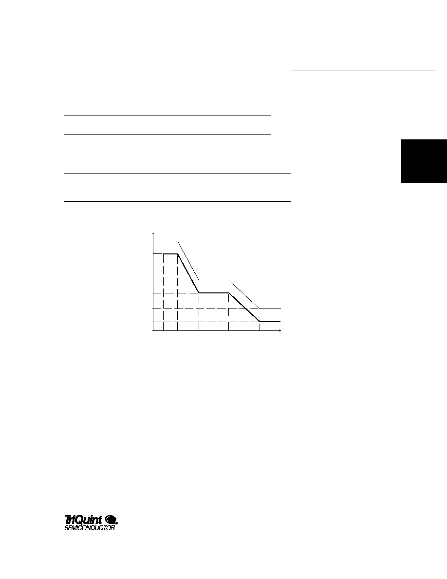
Figure 4. Jitter Tolerence
UI
pp
Frequency (Hz)
SONET/SDH
Template
15
1.5
0.3
0.15
3.0
30
100
600
6k
100k
1M
TQ8223 CDR
Table 9. Jitter Tolerence Performance
Symbol
Description
J
tolerence
The TQ8223 CDR exceeds the SONET/SDH Jitter Tolerence Template
according to the figure below.
Note: The method used to measure Jitter
Tolerence is outlined in a Jitter Bench
application note available upon request.

14
TQ8223
PRELIMINARY DATA SHEET
Figure 5. Typical Jitter Transfer Curve
Gain (dB)
Frequency (Hz)
Table 10. Jitter Transfer Performance
Symbol
Description
Nom
Max
Units
J
peaking
Peak Gain in Transfer Curve
0.05
0.1
dB
f
c
Corner Frequency Transfer Curve
1.76
2.0
MHz
Note: Jitter Transfer measurments were
performed with the PLL loop filter values
specified in Table 5. The method used is
outlined in a Jitter Bench application note
available upon request. The values listed as
nominal were performed under the following
conditions: VDD = 5 V
Tcase = 60 C
-40
-35
-30
-25
-20
-15
-10
-5
0
1.E+01
1.E+02
1.E+03
1.E+04
1.E+05
1.E+06
1.E+07
1.E+08
SONET/SDH Template
Transfer, 5.0V, 50C

TQ8223
15
SONET/SDH/A
TM
PRODUCTS
PRELIMINARY DATA SHEET
TELECOM
PRODUCTS
Signal
Symbol
Description
Min
Nom
Max
Units
DIN
V
dp-p
(N)DIN outer eye differential pk-pk amplitude
1000
1600
mV
pp
NDIN
(N)DIN data rate
2.48832
Gb/s
V
sens
Data channel sensitivity (Note 1)
40
mV
V
off
(N)DIN differential offset voltage
-25
+25
mV
T
dead
Data channel dead band (Note 2)
125
ps
V
hys
Data channel hysteresis (Note 3)
5
mV
Note 1:
Measured as the minimum inner eye amplitude of the data signal at DIN that can be correctly regenerated. Input clock/data phase
and Data decision threshold optimized for sensitivity.
All specifications apply under the following conditions.
Input data pattern:
2
23
-1 PRBS
Input data rate:
2.48832 Gbps
Input clock frequency:
2.48832 GHz
Input data rise/fall time (20 %/80 %) >100 ps
Note 2:
Measured as the input clock/data phase range over which errors can be detected at RQ11-18 in 1:8 mode. Specification
applies under the following conditions:
- input data amplitude: < 375mV mean
1
-mean
0
- Input data rise/fall time (20 %/80 %) >100 ps
Note 3:
Hysteresis is the difference in the decision threshold that results in error free operation of the channel when the decision threshold is
first increased and then decreased and vice versa starting from a level that results in error free operation of the channel. The
hysteresis specification applies for both the `1' and `0' signal levels. The DIN input conditions are the same as those listed in note 1
above.
Note 4:
All amplitudes are differential peak-peak voltage
Table 11. Data Channel Specifications (Note 4)

16
TQ8223
PRELIMINARY DATA SHEET
Signal
Symbol
Description
Min
Nom
Max
Units
CK78T
tckdc
Output clock duty cycle (Note 3)
40
50
60
%
tckr
Output clock rise time (20% to 80%)
2000
ps
tckf
Output clock fall time (20% to 80%)
2000
ps
Voh
Output clock high level
2.4
V
DD
V
Vol
Output clock low level
V
EE
0.4
V
Cload
Output load capacitance
20
pF
RQ11-18 Tpd1
Output data delay 1 (Note 1)
1.8
ns
RQ21-28 Tpd2
Output data hold time (Note 1)
0
ns
RQ31-38 Voh
Output high voltage (Note 2)
2.4
V
DD
V
RQ41-48 Vol
Output low voltage (Note 2)
V
EE
0.4
V
RQPAR1
Ioh
Output high-level output current
50
mA
RQPAR2
Iol
Output low-level output current
-20
mA
RQPAR3
Cload
Output load capacitance
20
pF
RQPAR4
LOCK
LOCKREF Vih
Input high level
2.0
V
DD
V
PPMSEL
Vil
Inputt low level
V
EE
0.8
V
MODE(0:1)
PARSEL
Notes:
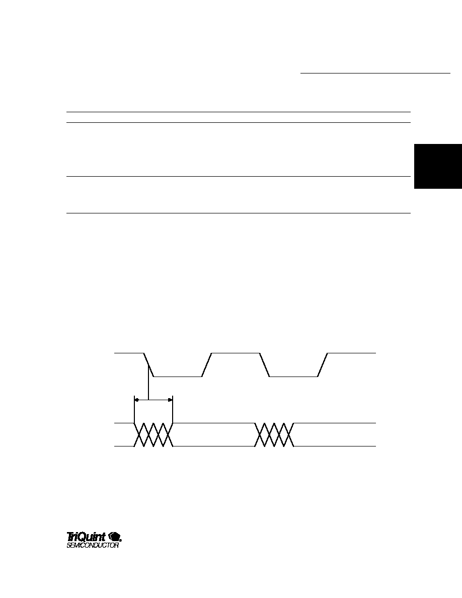
1.See Figure 6. Tpd1 and Tpd2 are specified relative to the falling edge of the CK78T signal. Output data edge jitter is not included in
the specifications. The output data streams are assumed to be free of any skewing in time. The specifications apply under the
following conditions:
Output data rise/fall time:
<= 2000ps (20% to 80%)
Output data:
2
23
-1 PRBS, 32x78Mb/s
Output clock frequency:
77.76MHz
2.Output data level requirements apply under the following conditions:
Output data:
2
23
-1 PRBS, 32x78Mbit/s
Output clock frequency:
77.76MHz
3.Output clock duty cycle is measured at the mean voltage of the signal and nominal input clock frequency of 2.48832GHz.
Table 12. TTL Interface Specifications

TQ8223
17
SONET/SDH/A
TM
PRODUCTS
PRELIMINARY DATA SHEET
TELECOM
PRODUCTS
T
pd2
T
pd1
Valid
Data
Valid
Data
Figure 6 AC Timing: 77.76 Mb/s TTL Interface
CK78T
RQ11-18
RQ21-28
RQ31-38
RQ41-48
Signal
Symbol
Description
Min Nom
(Note 4)
Max
Units
CK311
tckdc
Output clock duty cycle (Note 2)
40
50
60
%
NCK311
tckr
Output clock rise time (20% to 80%)
750
ps
CK155
tckf
Output clock fall time (20% to 80%)
750
ps
CK39
Voh
Output clock high level
V
DD
-1.0
-
V
DD
-0.6
V
(Note 1)
Vol
Output clock low level
V
TTe
-
V
DD
-1.6
V
Vamp
Output clock amplitude (Note 3)
+/-350
-
-
mV
SLIP
Vih
Input high level
V
DD
-1.05
V
DD
-0.4
V
RESET
Vil
Input low level
V
TTe
V
DD
-1.55 V
RSNT
tif
Input fall time (20% to 80%)
750
ps
HINTCLK tif
Input fall time (20% to 80%)
750
ps
Notes:
1.All specifications apply with signals terminated with R
Te
to V
TTe
.
2.Output clock duty cycle is measured at the mean voltage of the signal and nominal input clock frequency of 2.48832 GHz.
3.The CK155 and CK39 clock output amplitude is measured with respect to the mean voltage of the signal.
4.All NOM specifications apply under the following conditions.
Input data pattern:
2
23
-1 PRBS
Input data rate:
2.48832 Gbps
Input clock frequency:
2.48832 GHz
Input data rise/fall time (20 %/80 %) >100 p
Table 13. PECL Interface Specifications

18
TQ8223
PRELIMINARY DATA SHEET
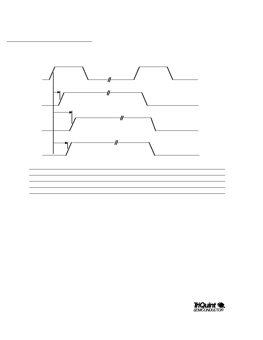
Table 14. Output Clock Timing Relationships
Symbol
Description
Typ
Max
Units
T
CK155
CK311 to CK155 timing relation
230
pS
T
CK78
CK311 to CK78 timing relation
1400
pS
T
CK39
CK311 to CK39 timing relation
700
pS
Figure 7. Output Clock Timing Relationships
CK311
CK155
CK78
CK39
T
CK155
T
CK78
T
CK39

TQ8223
19
SONET/SDH/A
TM
PRODUCTS
PRELIMINARY DATA SHEET
TELECOM
PRODUCTS
VEE
+2.2V
+5.0V
2.5GHz clock monitor
38.88MHz PECL clock
2.48832Gb/s from AGC
A.C.
Terminated
N.C. or VEE (GND)
38.88MHz clock
CLKSEL
LOCK
CK39
HCKOUT
MODE0
MODE1
N.C.
VOSC
VTUNE
VTUNE0
DATINV
DIN
VTD1
VTD2
NCKIN
HINTCLK
CKIN
VDD
Figure 8. 1:32 Demultiplexing with Internal PLL
Typical Application
PHADJ
Phase control from DAC
VEE
VDD
NDIN
VEE
N.C.
RQ1(1:8)
RQ4(1:8)
RQ2(1:8)
RQPAR1
RQ3(1:8)
RQPAR4
RQPAR2
CK78T(0:3)
RQPAR3
77.76Mb/s TTL Inter
face

20
TQ8223
PRELIMINARY DATA SHEET
VEE
+2.2V
+5.0V
2.5GHz clock monitor
38.88MHz clock
N.C.
VEE (GND)
2.48832Gb/s from AGC
N.C.
e
A.C.
Terminated
N.C. or VEE (GND)
38.88MHz clock
RQ1(1:8)
RQ4(1:8)
RQ2(1:8)
RQPAR1
RQ3(1:8)
RQPAR4
RQPAR2
CK78T(0:3)
RQPAR3
CLKSEL
CK39
HCKOUT
MODE0
MODE1
RSTN
VOSC
DCREF
PHADJ
DATINV
PHREF
DIN
VTD1
VTD2
NCKIN
CKIN
VEE
VDD
Figure 9. 1:32 Demultiplexing with Internal VCO and External PLL
VTUNE
77.76Mb/s TTL Inter
face
Phase control from DAC
NDIN
HINTCLK
VDD

TQ8223
21
SONET/SDH/A
TM
PRODUCTS
PRELIMINARY DATA SHEET
TELECOM
PRODUCTS
Top view
Bottom view
Side View Section
D
E
A1 Ball I.D. Mark
45
o
0.5mm Chamfer
A
B
C
D
E
F
G
H
J
K
L
M
N
P
R
T
U
17 16 15 14 13 12 11 10 9 8 7 6 5 4 3 2 1
D1
E1
e
e
b
A1 Ball
Corner
A
A1
C
aaa
P
Figure 10. 208-pin BGA Mechanical Dimensions
Symbol
Parameter
Min
Nom
Max
A
Overall Thickness
1.45
1.55
1.65
A1
Ball Height
0.60
0.65
0.70
D
Body Size
22.80
23.00
23.20
D1
Ball Footprint
20.32 (BSC.)
E
Body Size
22.80
23.00
23.20
E1
Ball Footprint
20.32 (BSC.)
b
Ball Diameter
0.65
0.75
0.85
c
Body Thickness
0.85
0.90
0.95
aaa
Seating Plane Clearance
0.15
e
Ball Pitch
1.27 TYP.
P
Encapsulation Clearance
0.15
Table 15. 208-pin BGA Dimensions
Note: Heat Spreader is at VDD volts.
Note: All dimensions in millimeters (mm)

22
TQ8223
PRELIMINARY DATA SHEET
The information provided herein is believed to be reliable; TriQuint assumes no liability for inaccuracies or
omissions. TriQuint assumes no responsibility for the use of this information, and all such information
shall be entirely at the user's own risk. Prices and specifications are subject to change without notice.
No patent rights or licenses to any of the circuits described herein are implied or granted to any third party.
TriQuint does not authorize or warrant any TriQuint product for use in life-support devices and/or systems.
Copyright © 1999 TriQuint Semiconductor, Inc. All rights reserved.
Revision 0.2.A
August 1999

