 | –≠–ª–µ–∫—Ç—Ä–æ–Ω–Ω—ã–π –∫–æ–º–ø–æ–Ω–µ–Ω—Ç: TQHBT3 | –°–∫–∞—á–∞—Ç—å:  PDF PDF  ZIP ZIP |

Production Process
TQHBT3
InGaP HBT Foundry Service
Features
∑
2≠ and 3-um emitter widths
∑
>22 dB MAG @ 6 GHz; with 3-um
emitters
∑
Amplifier Ruggedness: VSWR 70:1
@ 5 V supply
∑
High Linearity in PA applications
∑
InGaP Emitter Process for High Re-
liability and Thermal Stability
∑
Base Etch Stop for Uniformity
∑
MOCVD Epitaxy
∑
High Density Interconnects;
∑
2 Global, 1 Local
∑
Over 6 µm Total Thickness
∑
Dielectric Encapsulated Metals
∑
Thick Metal Interconnects:
∑
Enhanced Thermal Management
∑
Minimum Die Size
∑
Effective Base Ballasting for Maxi-
mum Gain
∑
150 mm Wafers
∑
High-Q Passives
∑
NiCr Thin Film Resistors
∑
High Value Capacitors & Stacked
Capacitors
∑
Backside Vias Optional
∑
Validated Models and Design
Support
Applications
∑
Power Amplifiers
∑
Driver Amplifiers
∑
Wideband, General Purpose
Amplifiers
General Description
TriQuint's new TQHBT3 process is a highly reliable InGaP
HBT process with three levels of interconnecting metal and
state-of-the-art device performance. Thick metal intercon-
nects and high quality passives promote integration. The thick
metal interconnects, which promote enhanced thermal man-
agement, and high density capacitors keep die sizes small.
MOCVD epitaxial processes are utilized to grow the active
layers. A carbon-doped Base and InGaP Emitter are utilized
for high RF performance consistent with high reliability. De-
signs utilizing the 3-um emitter width have the performance of
previous 2-um emitters, but with the reliability and ruggedness
associated with wider emitters. Precision NiCr resistors and
high value MIM capacitors are included. The three metal layers
are encapsulated in a high performance dielectric that allows
wiring flexibility and plastic packaging simplicity.
Semiconductors for Communications
www.triquint.com
TriQuint Semiconductor
2300 NE Brookwood Pkwy
Hillsboro, Oregon 97124
Phone: 503-615-9000
Fax: 503-615-8905
Email: info@triquint.com
Page 1 of 6; Rev 1.1 2/8/2005
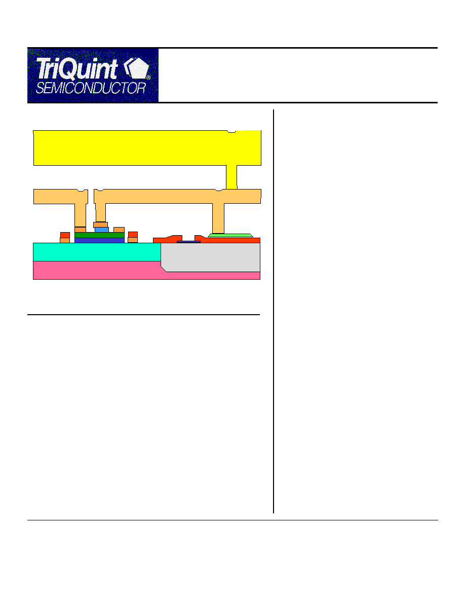
TQHBT3 Process Cross-Section
Dielectric
Metal 2 - 4um
Dielectric
MIM
NiCr
Metal 0
C
C
B
B
E
Emitter
Base
Collector
Sub Collector
Buffer & Substrate
Isolation Implant
Metal 1 - 2um
Metal 1 - 2um
Dielectric
Metal 2 - 4um
Dielectric
MIM
NiCr
Metal 0
C
C
B
B
E
Emitter
Base
Collector
Sub Collector
Buffer & Substrate
Isolation Implant
Metal 1 - 2um
Metal 1 - 2um
Dielectric
Metal 2 - 4um
Dielectric
MIM
NiCr
Metal 0
C
C
B
B
E
Emitter
Base
Collector
Sub Collector
Buffer & Substrate
Isolation Implant
Metal 1 - 2um
Metal 1 - 2um
Dielectric
Metal 2 - 4um
Dielectric
MIM
NiCr
Metal 0
C
C
B
B
E
Emitter
Base
Collector
Sub Collector
Buffer & Substrate
Isolation Implant
Metal 1 - 2um
Metal 1 - 2um

Production Process
TQHBT3
InGaP HBT Foundry Service
Semiconductors for Communications
www.triquint.com
TriQuint Semiconductor
2300 NE Brookwood Pkwy
Hillsboro, Oregon 97124
Phone: 503-615-9000
Fax: 503-615-8905
Email: info@triquint.com
Page 2 of 6; Rev 1.1 2/8/2005
TQHBT3 Process Details
Element
Parameter
Value
Units
HBT Transistor
Emitter Periphery
(Standard Cell)
3 x 3 x 30
µm
Vbe
1.15
V
Beta
130
Ft
40
GHz
Fmax
65
GHz
BVcbo
24
V
BVbeo
7
V
BVceo
14
V
Interconnect
Metal Layers
3
MIM Caps (Top
Stacked Cap)
Value
1200
pF/mm2
Inductors
Q @ 2 GHz
>20
Resistors
NiCr
50
Ohms/sq
Bulk
350
Ohms/sq
Vias
Yes
Mask Layers
No Vias
14
With Vias
16
2um emitters are also available!
Bottom Stacked Cap
Value
625
pF/mm2
TQHBT3
Process
Details
HBT Storage Temperature Range
-65 to +150
Deg C
HBT Operating Junction Temperature Range
-55 to +150
Deg C
Junction Current Denstity
20
kA/cm^2
20
V
MIM Capacitor
Maximum
Ratings

Production Process
TQHBT3
InGaP HBT Foundry Service
Semiconductors for Communications
www.triquint.com
TriQuint Semiconductor
2300 NE Brookwood Pkwy
Hillsboro, Oregon 97124
Phone: 503-615-9000
Fax: 503-615-8905
Email: info@triquint.com
Page 3 of 6; Rev 1.1 2/8/2005
TQHBT3
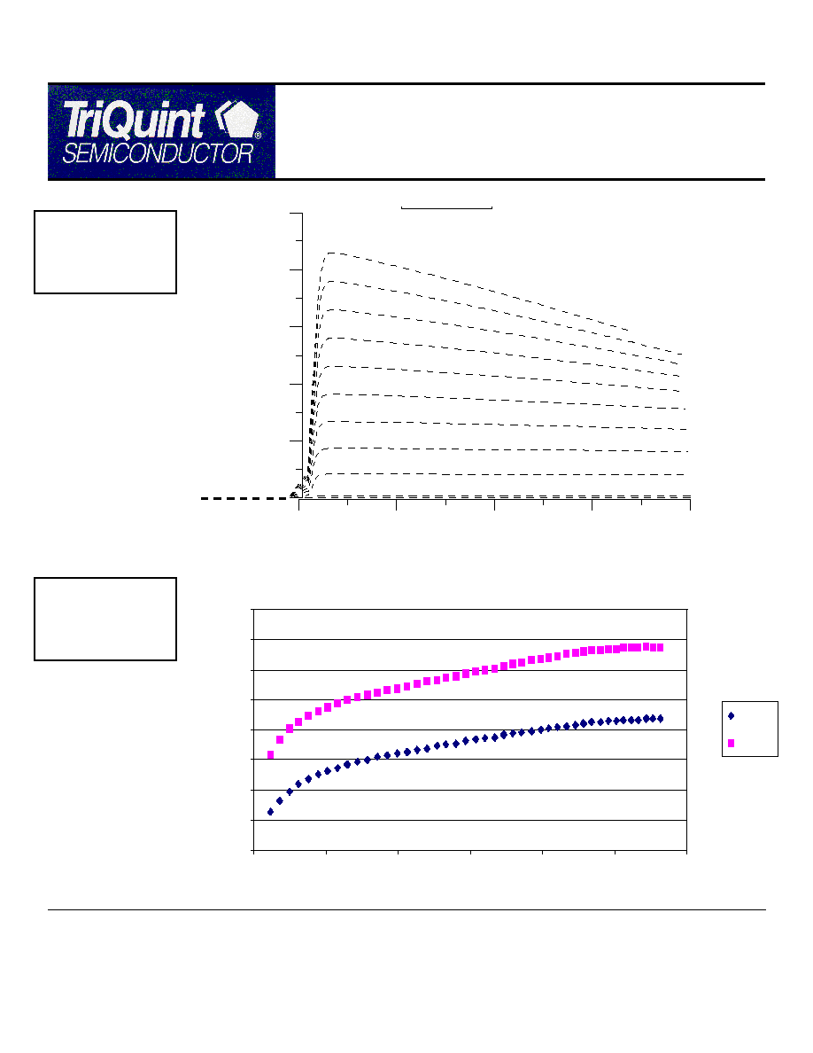
DC I--V Plot
Ft, Fmax vs Ic
@Vce=3.5V
0
2
4
6
8
Vce (V)
0
0.02
0.04
0.06
0.08
0.1
Ic
(
A
)
Device size: 3X3X30
Ib=0.7uA to Ib=600uA,
step size=67uA
0
10
20
30
40
50
60
70
80
0.00E+00
5.00E-02
1.00E-01
1.50E-01
2.00E-01
2.50E-01
3.00E-01
Ic (mA/um^2)
Fr
equency (
G
Hz)
Ft
Fmax

Production Process
TQHBT3
InGaP HBT Foundry Service
Semiconductors for Communications
www.triquint.com
TriQuint Semiconductor
2300 NE Brookwood Pkwy
Hillsboro, Oregon 97124
Phone: 503-615-9000
Fax: 503-615-8905
Email: info@triquint.com
Page 4 of 6; Rev 1.1 2/8/2005
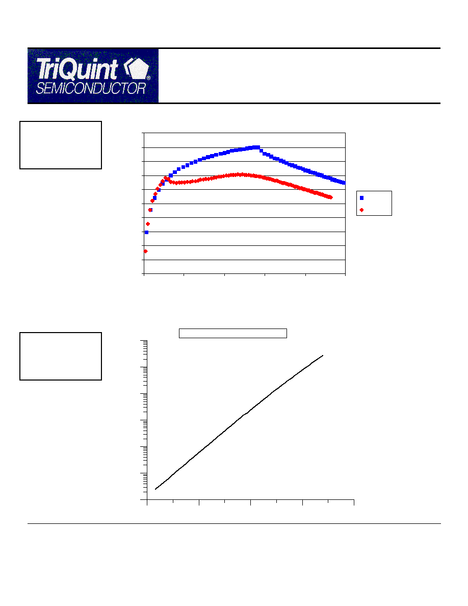
Gain at 6.1 GHz
Versus
Current Density
Gummel Plot of
TQHBT3
5
7
9
11
13
15
17
19
21
23
25
0
10
20
30
40
50
Ic (kA/cm2)
G
a
in (
d
B)
3x3x30
3x3x45
1
1.1
1.2
1.3
1.4
Vbe(V)
1E-007
1E-006
1E-005
0.0001
0.001
0.01
0.1
Ic
(
A
)
Gummel Plot (Ic vs Vbe)
Device size:3X3X30

Production Process
TQHBT3
InGaP HBT Foundry Service
Semiconductors for Communications
www.triquint.com
TriQuint Semiconductor
2300 NE Brookwood Pkwy
Hillsboro, Oregon 97124
Phone: 503-615-9000
Fax: 503-615-8905
Email: info@triquint.com
Page 5 of 6; Rev 1.1 2/8/2005
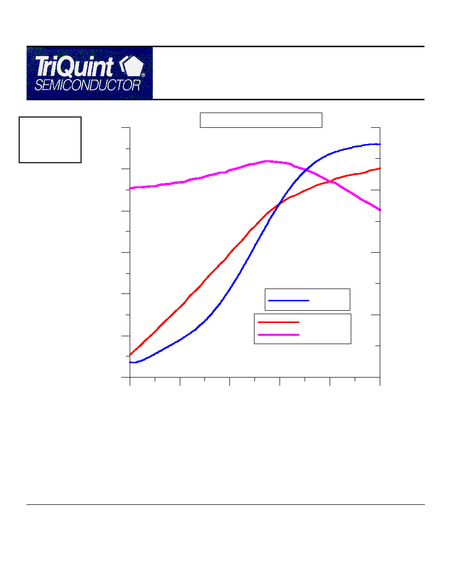
CW
@ 1.9 GHz
-20
-15
-10
-5
0
5
-5
0
5
10
15
20
25
Gain(
dB
), P
o
ut(
d
Bm
)
0
20
40
60
80
Pout(dBm)
Gain (dB)
-20
-15
-10
-5
0
5
Pin (dBm)
P
A
E
(
%
)
PAE(%)
Gain, Pout, PAE vs Pin
Device size: 3X3X30
Freq=1.9GHz
Vce=3.4V, Ic=3.3mA
Load Gamma @ 1.9GHz = 0.43<24.7
Source Gamma @ 1.9GHz = 0.62<164.7
Load Gamma @ 3.8GHz = 0.59<-171.6
Source Gamma @ 3.8GHz = 0.71<17.1

Production Process
TQHBT3
InGaP HBT Foundry Service
Semiconductors for Communications
www.triquint.com
TriQuint Semiconductor
2300 NE Brookwood Pkwy
Hillsboro, Oregon 97124
Phone: 503-615-9000
Fax: 503-615-8905
Email: info@triquint.com
Page 6 of 6; Rev 1.1 2/8/2005
Applications Support Services
∑
Tiling of GDSII Stream Files including PCM
∑
Design Rule Check Services
∑
Layout versus Schematic Check Services
∑
Packaging Development Engineering
∑
Test Development Engineering:
∑
On-Wafer
∑
Packaged Parts
∑
Thermal Analysis Engineering
∑
Yield Enhancement Engineering
∑
Part Qualification Services
∑
Failure Analysis
Manufacturing Services
∑
Mask Making
∑
150 mm Wafer Fab
∑
Wafer Thinning
∑
Wafer Sawing
∑
Substrate Vias
∑
DC Die Sort Testing
∑
RF On-Wafer Testing
∑
Plastic Packaging
∑
RF Packaged Part Testing
Please contact your local TriQuint Semiconductor Representative/ Distributor
or Foundry Services Division Marketing for Additional information:
E-mail: sales@triquint.com
Phone: (503) 615-9331
Fax: (503) 615-8905
Design Tool Status
∑
Design Manual
∑
Device Library of Circuit Elements: Transistors, Diodes,
Thin Film Resistors, Capacitors, Inductors
∑
Parameters for 2nd-generation, TriQuint-Modified Gummel-
Poon Model Available Now
∑
Agilent ADS & AWR MWO
∑
Process Variation Models available now
∑
Layout Files Available for:
∑
ICED & Cadence
∑
Layout Rule Sets for Design Rule & Layout versus Schematic
Check Available:
∑
ICED & Cadence
∑
Qualified Package Models for Supported Package Styles
Prototyping and Development
∑
Prototype Development QuickTurn (PDQ):
∑
Shared Mask Set;
∑
Run Monthly
∑
Hot Lot Cycle Time
∑
Via and Non-Via Options
∑
Prototype Wafer Option (PWO):
∑
Customer-specific Masks, Customer Schedule
∑
2 wafers delivered
∑
With thinning and sawing; optional backside vias
Process Qualification Status
∑
Process based on TQHBT2.5 production process.
∑
Full wafer level, process and packaged part qualification
complete for TQHBT3. Contact TriQuint for relevant
reports.
∑
For more information on Quality & Reliability, contact
TriQuint or visit:
www.triquint.com/manufacturing/QR/
Training
∑
GaAs Design Classes:
∑
Half Day Introduction; Upon Request
∑
Four Day Technical Training; Fall & Spring at
TriQuint Oregon facility
∑
For Training & PDQ Schedules please visit:
www.triquint.com/foundry/
