 | –≠–ª–µ–∫—Ç—Ä–æ–Ω–Ω—ã–π –∫–æ–º–ø–æ–Ω–µ–Ω—Ç: TQHBTr21 | –°–∫–∞—á–∞—Ç—å:  PDF PDF  ZIP ZIP |

0.5-µm
Low-Noise, Low-Current
MesFET (LNLC)
Process Data Sheet
Semiconductors for Communications, Space and Military
www.TriQuint.com
500 West Renner Road
Richardson, Texas 75080
Phone: 972-994-8200
Foundry: 972-994-4545
Email: info@triquint.com
Page 1 of 3; 9/24/02
Specifications are subject to change.
General Description
The 0.5-µm Low-Noise, Low-Current MesFET (LNLC)
process is a cost-effective 2MI (2-metal-interconnect) de-
pletion-mode ion-implant MesFET process for low-noise
applications through 20 GHz. The LNLC process allows
for switch, amplifier and diode integration and is used
mainly in low-noise amplifier applications such as receivers.
Passives include 2 thick-metal interconnect layers, preci-
sion TaN resistors, GaAs resistors, MIM capacitors, and
through-substrate vias. The via-under-cap process aides in
size compaction and offers excellent grounds at higher fre-
quencies.
Features
∑
0.5-µm amplifier transistors
∑
0.5-µm switch transistors
∑
0.5-µm diodes
∑
Device passivation
∑
High-Q passives
∑
MIM capacitors
∑
TaN resistors
∑
GaAs resistors
∑
2 metal layers
∑
Air bridges
∑
Substrate vias
∑
Operation up to V
d
= 5 V
Applications
∑
Up to 20 GHz
∑
Communications
∑
Space
∑
Military
∑
Low-noise amplifiers
∑
Driver amplifiers
∑
AGC amplifiers
∑
Limiting amplifiers
∑
Transimpedance amplifiers
∑
Differential amplifiers
∑
Digital and analog phase shifters
∑
Digital and analog attenuators
∑
Mixers (up and down converters)
∑
Multipliers
∑
Switches
∑
Oscillators
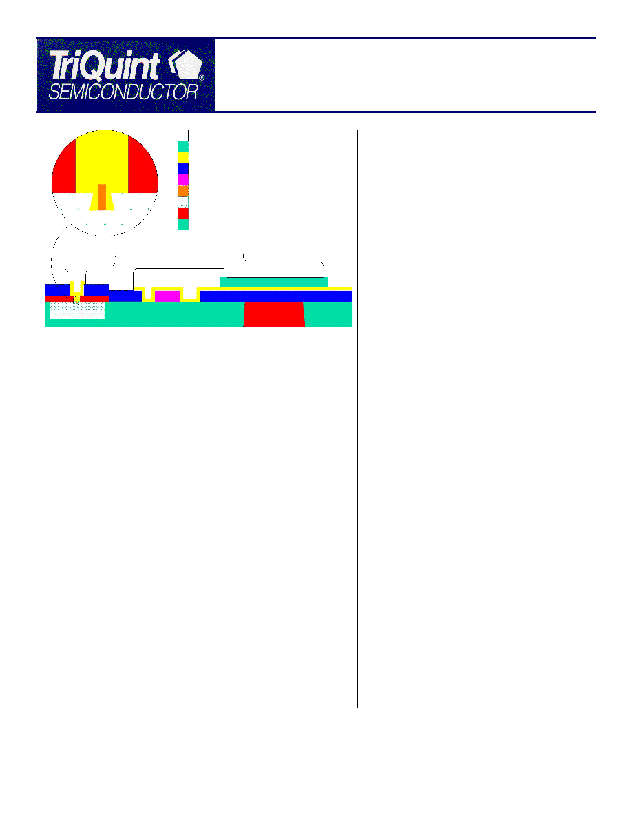
4.6 µm PLATING
CAP TOP PLATE
2000 ≈ NITRIDE
0.75 µm FIRST METAL
TaN RESISTOR
GATE
ACTIVE REGION
OHMIC METAL (EXCEPT VIA)
SEMI-INSULATING GaAs SUBSTRATE
VIA UNDER CAP
0.5-µm 2MI Process Cross Section

0.5-µm
Low-Noise, Low-Current
MesFET (LNLC)
Process Data Sheet
Semiconductors for Communications, Space and Military
www.TriQuint.com
500 West Renner Road
Richardson, Texas 75080
Phone: 972-994-8200
Foundry: 972-994-4545
Email: info@triquint.com
Page 2 of 3; 9/24/02
Specifications are subject to change.
Application Examples
DC to 14 GHz Power Amplifier TGA8349-SCC:
The TriQuint TGA8349-SCC is a GaAs monolithic low-noise distributed amplifier designed for use
as a multi-octave general-purpose gain block. The device provides 3.1 dB noise figure at mid-
band. Typical power output is 16 dBm at 1-dB gain compression.
2 to 20 GHz Low-Noise Amplifier TGA8310-SCC:
The TriQuint TGA8310-SCC is a monolithic low-noise distributed amplifier, which operates from 2
to 20 GHz. Typically, noise figure is 4 dB with a small signal gain of 9 dB. This low-noise
distributed amplifier is suitable for a variety of wideband electronic warfare systems such as radar
warning receivers, electronic counter measures, decoys, jammers and phased array systems.
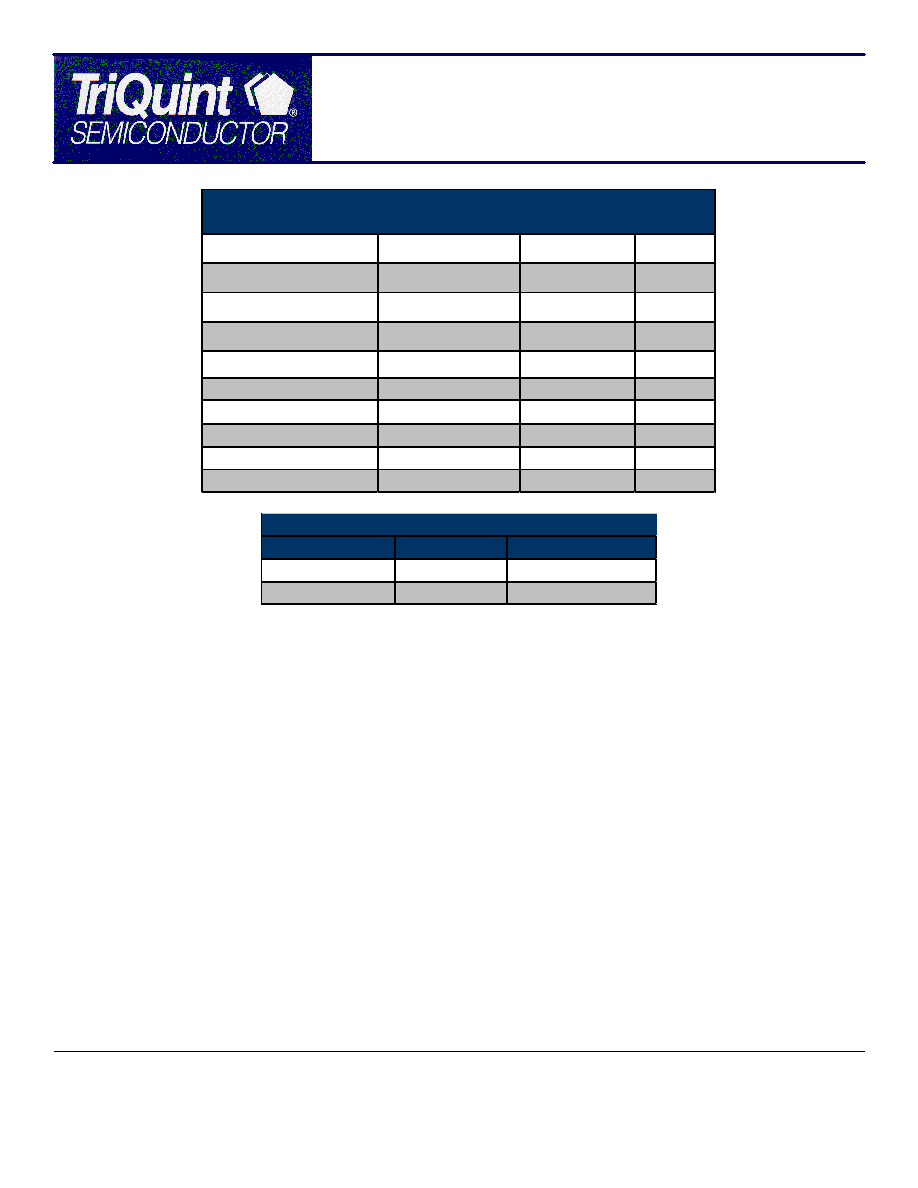
Gate Pitch (µm) Gate Fingers FET Sizes (µm)
26 26
4
300
26 26
8
300
FET Models Available (Noise)
Element
Parameter
Typical Value
Units
FETs
I
dss
190
mA/mm
G
m
240
mS/mm
V
bd
-13
V
V
p
-1.15
V
MIM capacitors
density
300
pF/mm
2
Capacitors over vias
yes
TaN resistors
sheet resistance
50
V
/sq
GaAs resistors
sheet resistance
370
V
/sq
Vias
yes
Substrate
thickness
100
µm
0.5-µm Low-Noise MesFET Process Details

0.5-µm
Low-Noise, Low-Current
MesFET (LNLC)
Process Data Sheet
Semiconductors for Communications, Space and Military
www.TriQuint.com
500 West Renner Road
Richardson, Texas 75080
Phone: 972-994-8200
Foundry: 972-994-4545
Email: info@triquint.com
Page 3 of 3; 9/24/02
Specifications are subject to change.
Prototyping and Development
∑
Prototype Wafer Option (PWO)
∑
Customer-specific masks
∑
Customer schedule
∑
2 wafers delivered
∑
Backside via process included
∑
PCM (process control monitor) qualified
wafers
Process Status
0.5-µm Low-Noise, Low-Current MesFET (LNLC)
is fully released and qualified
Contact TriQuint or visit
http://www.triquint.com/company/quality/
for more information on quality and reliability.
Manufacturing Services
∑
Mask making
∑
Wafer thinning
∑
Wafer dicing
∑
Substrate vias
∑
DC die-sort testing
∑
RF die-sort testing
∑
Final visual inspection
Design Tools
∑
Device libraries of circuit elements:
∑
FETs
∑
Thin-film and implanted resistors
∑
Capacitors
∑
Inductors
∑
Agilent ADS design kit
∑
MASC Library
Training
∑
GaAs design classes:
∑
Half-day introduction upon request
∑
3-day technical training upon request at
the TriQuint Texas facility
.
Applications Services
∑
Tiling of GDSII stream files including PCM
(process control monitor)
∑
Design rule checking
∑
Layout versus schematic checking
∑
Engineering:
∑
On-wafer DC test
∑
On-wafer RF test
∑
Thermal analysis
∑
Yield enhancement
∑
Part qualification
∑
Failure analysis
∑
Space qualification


