�
Triscend A7S Configurable
System-on-Chip Platform
August, 2002
(Version 1.10)
Product Description
� 2000-2002 by Triscend Corporation. All rights reserved.
TCH305-0001-002
Patents Pending.
!
Industry's first complete 32-bit Configurable
System-on-Chip (CSoC)
� High-performance, low-power consumption,
32-bit RISC processor (ARM7TDMITM)
� 8Kbyte mixed instruction/data cache
� 16Kbyte internal scratchpad RAM
� Next-generation embedded programmable
logic architecture (up to 25,600 ASIC gates)
� High-performance dedicated internal bus
(up to 455Mbytes per second at 60 MHz)
� External memory interface supporting
Flash, EEPROM, SRAM, and SDRAM
� Advanced real-time, in-system debugging
capability
� Stand-alone operation from a single
external memory (code + initialization)
� 2.5-volt core with 3.3- or 2.5-volt I/Os
� Four independent high-performance DMA
channels
!
High-performance, 32-bit
ARM7TDMI RISC Processor
� Popular, industry-standard 32-
bit RISC processor
� Binary and source code
compatible with other ARM7/ARM7TDMI
variants
� Widespread C/C++ compiler, source-level
debugger, and RTOS support
� Superior code density using the
Thumb
�
instruction set
� 54 MIPS (Dhrystone 2.1) at 60 MHz
� Low latency, real-time interrupt response
� Fast hardware multiplier
� 32-bit register bank and ALU
� 32-bit addressing 4Gbyte linear address
� 32-bit barrel shifter
� EmbeddedICETM on-chip debugger
Configurable
System Logic
(CSL)
matrix
PIO
PIO
PIO
PIO
PIO
CSI Bus
Arbiter
Power Control
Address Bus
Selector
Selector
Clock Synthesizer
Power-On Reset
To external memory
Configurable System
Interconnect (CSI) bus
Configurable System
Interconnect socket
Selector
Selector
Selector
Four-channel
DMA Controller
JTAG Interface
Hardware
Breakpoint Unit
Memory Interface
Unit
SDRAM Controller
Static/Flash Interface
Selector
PIO
PIO
PIO
Cache
* 8K Bytes
* 4-way Set Associative
* Protection Unit
CSI Bridge
16KBytes
ScratchPad
SRAM
or
Trace Buffer
Data Bus
Local CPU Bus
ARM7TDMI
16-bit
Timer
32-bit
Watchdog Timer
16-input
Interrupt Controller
16-bit
Timer
UART
with FIFO
UART
with FIFO
Standard Peripherals
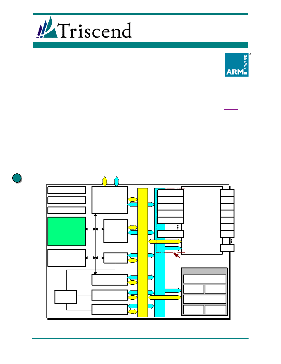
Figure 1. Block diagram of the Triscend A7S Configurable System-on-Chip (CSoC).
?

Triscend A7S Configurable System-on-Chip Platform
SUBJECT TO CHANGE
2
TCH305-0001-002
!
Rich set of embedded support peripherals
� 4-channel high-performance DMA controller
� fly-by performance
� memory-to-memory transfers
� linked-list DMA
� frame transfer support
� Memory Subsystem Interface Unit (MSSIU)
for flexible, glueless interface to external
memories (ROM, EEPROM, Flash, SRAM,
and SDRAM)
� Two 16C550-style serial ports (UART) with
modem interface
� Two 16-bit timers/counters
� 32-bit Watchdog timer
� 16-input interrupt controller with fast
interrupt response
� IEEE 1149.1 enhanced JTAG interface
� In-system debug/breakpoint unit
� Power-on reset
� Power-down and power-management
modes
!
Full-Featured Memory Interface Unit
� Simultaneous support for independent
external Flash and SDRAM memory sub-
systems using x8 or x16 memory devices
� Expandable external data bus: 8-bit, 16-bit
and 32-bit support
� Up to two external SDRAM banks
� Automatic support for self-refresh, auto-
refresh and initialization of SDRAM
� Programmable SDRAM parameters for
optimal memory bandwidth
!
Embedded SRAM-based Configurable Sys-
tem Logic (CSL) matrix
� Next-generation embedded programmable
logic architecture, optimized with processor
and bus interface
� Over 2,600 flip-flops and 190 programma-
ble inputs and outputs (PIOs)
� Abundant, flexible interconnect structure
with easy access to and from system bus
� Dedicated circuitry for fast adders,
counters, and multipliers
� CSL cells optionally used as distributed
memory, including true dual-port operation
� Six independent low-skew clock or global
signal distribution buffers plus bus clock
� Supported by standard logic design tools
� VHDL and Verilog logic synthesis
� Schematic entry
� VHDL and Verilog simulation
!
High performance dedicated system bus
� Configurable System Interconnect (CSI)
bus integrates CSL matrix, CSoC system
� 455Mbytes per second peak transfer rate
� 32-bit address bus and 32-bit data bus
� Programmable wait-state support
� Openly-defined CSI Socket bus interface to
CSL matrix
� CSL peripheral addresses independent
of placement in CSL matrix
� CSL peripherals compatible with past
and future CSoC families
� Ten bus masters and built-in arbitration
� ARM7TDMITM CPU
� Four-channel DMA controller
� JTAG interface
Table 1. Triscend A7S Configurable System-on-Chip Family
Device
Embedded
Processor
Core
Dedicated
Resources
System
RAM
Configurable
System Logic
(CSL) Cells
CSI
Address
Selectors
PIO*
Pins
(Max)
TA7S04 448
32
124
TA7S20
ARM7TDMI
32-bit RISC CPU
8K unified cache
Barrel shifter
Hardware multiplier
Thumb extensions
Debug extensions
Flash memory interface
SDRAM memory interface
4-channel DMA controller
Two 16C550-style UARTs
Two 16-bit timers
32-bit watchdog timer
16-input interrupt controller
Power management
Power-on reset
Hardware breakpoint unit
JTAG debugger
4Kx32
2,048 128
252
* Maximum PIO on each base device, actual PIO count depends on package style and initialization mode. See
Table 61
.

TCH305-0001-002
3
SUBJECT TO CHANGE
System Overview
The Triscend A7S Configurable System-on-Chip (CSoC) device is a complete, high-
performance user-programmable system. The A7S contains
#
an embedded 32-bit ARM7TDMI RISC processor
#
a next generation embedded programmable logic architecture, optimized for processor
and bus interface
#
a high-performance 32-bit internal bus supporting up to 455Mbytes per second peak
transfer rates
#
16Kbytes of internal scratchpad SRAM memory and a separate 8Kbyte cache.
The ARM7TDMI is a general-purpose 32-bit RISC microprocessor that supports the com-
plete ARM 32-bit instruction set and the reduced 16-bit instruction set, referred to as
Thumb. The ARM7TDMI processor offers the following advantages:
#
High-performance for very low power consumption and price
#
Excellent code density using the Thumb instruction set
#
Low-latency interrupt response
A
A
R
R
M
M
7
7
T
T
D
D
M
M
I
I
P
P
r
r
o
o
c
c
e
e
s
s
s
s
o
o
r
r
S
S
y
y
s
s
t
t
e
e
m
m
w
w
i
i
t
t
h
h
C
C
a
a
c
c
h
h
e
e
,
,
S
S
c
c
r
r
a
a
t
t
c
c
h
h
p
p
a
a
d
d
R
R
A
A
M
M
The processor is paired with an 8Kbyte unified code/data cache and a 16Kbyte (4Kx32)
scratchpad RAM for storing timing critical code or data. The scratchpad is accessible over
the Configurable System Interconnect (CSI) bus by other CSI bus masters, primarily for
DMA transfers. The ARM processor is integrated with other system components and the
Configurable System Logic (CSL) matrix to provide a complete configurable system, as il-
lustrated in
Figure 1
.
N
N
e
e
x
x
t
t
-
-
G
G
e
e
n
n
e
e
r
r
a
a
t
t
i
i
o
o
n
n
E
E
m
m
b
b
e
e
d
d
d
d
e
e
d
d
P
P
r
r
o
o
g
g
r
r
a
a
m
m
m
m
a
a
b
b
l
l
e
e
L
L
o
o
g
g
i
i
c
c
A
A
r
r
c
c
h
h
i
i
t
t
e
e
c
c
t
t
u
u
r
r
e
e
The embedded SRAM-based Configurable System Logic (CSL) matrix provides full, easy-
to-use system customization. The high-performance programmable logic architecture
consists of a highly interconnected matrix of CSL cells. Resources within the matrix pro-
vide seamless access to and from the internal CSI bus. Each CSL cell performs various
potential functions, including combinatorial and sequential logic. The combinatorial por-
tion performs Boolean logic operations, arithmetic functions, and memory. The sequential
element performs independently or in tandem with the combinatorial function. The abun-
dant programmable input/output blocks (PIOs) provide a highly flexible interface between
external functions and the internal system bus or configurable system logic. Each PIO of-
fers advanced I/O capabilities including selectable output drive current, optional input hys-
teresis, and programmable low-power functionality during power-down mode.
I
I
n
n
t
t
e
e
r
r
n
n
a
a
l
l
,
,
H
H
i
i
g
g
h
h
-
-
P
P
e
e
r
r
f
f
o
o
r
r
m
m
a
a
n
n
c
c
e
e
B
B
u
u
s
s
A high-performance internal system bus--called the Configurable System Interconnect
(CSI) bus-- interconnects the embedded processor, its peripherals, and the CSL matrix at
a maximum speed of 60MHz. The bus simultaneously provides 32 bits of read data, 32
bits of write data, and a 32-bit address. Multiple bus masters arbitrate for bus access.
Potential bus masters include the ARM7TDMI processor, the read and write channels of
all four DMA channels, and the JTAG interface. CSL-based devices become CSI bus
masters using DMA services. The CSI bus and the local CPU bus following the little en-
dian format.

Triscend A7S Configurable System-on-Chip Platform
SUBJECT TO CHANGE
4
TCH305-0001-002
E
E
x
x
t
t
e
e
r
r
n
n
a
a
l
l
I
I
n
n
t
t
e
e
r
r
f
f
a
a
c
c
e
e
t
t
o
o
F
F
l
l
a
a
s
s
h
h
,
,
S
S
D
D
R
R
A
A
M
M
A static memory interface unit seamlessly connects the A7S device to external static
memories such as Flash or SRAM, as shown in
Figure 2
. An external Flash memory de-
vice contains the A7S's initialization boot program plus the system application code. The
external memory interface has programmable read/write control and chip-select signals
that provide flexible set-up, strobe, and hold timing. The CPU connects directly to exter-
nal memory, eliminating any potential latency incurred by using the CSI bus. For low fre-
quency or minimal applications, the ARM7TDMI processor directly fetches its instructions
from external Flash.
The A7S optionally supports external SDRAM, offering additional affordable and high-
density memory to the system. The SDRAM interface connects an A7S-based system to
a variety of SDRAM types and configurations, including 100-pin DIMMs. The SDRAM in-
terface operates at up to 60 MHz and provides options to optimize the interface timing for
slower system clocks. SDRAM memory is ideal for DMA buffers. Similarly, the applica-
tion program can be stored in slow, cheap, byte-wide Flash and copied into SDRAM at
power-up. Then, the CPU starts executing code from the wider and faster SDRAM mem-
ory. The Flash and SDRAM interfaces share device pins, as shown in
Figure 2
.
Triscend A7
Configurable
System-on-Chip
(CSoC)
JTAG Connector
TCK TMS
TDI
TDO
TCK TMS
TDI
TDO
XIN
XOUT
RST-
SLAVE-
VCCIO
VCCIO
PIO[xxx:0]
FLASH
1Mx8
CE-
WE-
OE-
A[19:0]
D[7:0]
CE0-
WE-
OE-
SDCE0-
SDCLK
SDCKE
D[7:0]
D[15:8]
D[23:16]
D[31:24]
A[19:0]
A[23:20]
A[31:24]
[1]
[0]
[0]
[1]
[3:2]
[5:4]
[7:6]
[7:6]
[18:8]
[18:8]
CSoC Initialization Data
Application Code Storage
Faster Code Fetch Store
Application Data Storage
SDRAM
4Mx16
RAS
CAS
CLK
CKE
BS[1:0]
DQM[1:0]
WE-
CE-
A[10:0]
DQ[15:0]
SDRAM
4Mx16
RAS
CAS
CLK
CKE
BS[1:0]
DQM[1:0]
WE-
CE-
A[10:0]
DQ[15:0]
32.768 kHz
(OPTIONAL)
(OPTIONAL)
VCCPLL
+2.5V
VCCIO
+2.5V
or
+3.3V
VSYS
To ext.
memory
supply
VCC
+2.5V
GNDPLL
GNDIO
GND
Figure 2. A typical A7S-based system.

TCH305-0001-002
5
SUBJECT TO CHANGE
F
F
o
o
u
u
r
r
-
-
C
C
h
h
a
a
n
n
n
n
e
e
l
l
D
D
M
M
A
A
The four-channel DMA controller provides high-bandwidth communication between CSL-
based I/O devices, at up to 228M bytes per second, per direction. The easy-to-use DMA
handshake simplifies interface and control logic within the CSL. The DMA controller pro-
vides advanced capabilities such as linked-list and frame-transfer support.
Dedicated Peripherals
The A7S also offers a set of common dedicated peripherals including
#
two 16-bit timers with pre-scalers,
#
two 16C450/550-like serial controllers (UART), with an optional modem interface
#
a 32-bit watchdog timer, and
#
an interrupt controller.
C
C
o
o
m
m
p
p
l
l
e
e
t
t
e
e
S
S
i
i
n
n
g
g
l
l
e
e
-
-
C
C
h
h
i
i
p
p
S
S
y
y
s
s
t
t
e
e
m
m
The majority of the system, including the CPU, operates from a single clock signal. The
clock source is typically driven directly via an external pin or connected to the on-chip PLL
clock synthesizer. The clock synthesizer operates from an external 32.768 kHz watch
crystal. Additionally, an internal ring oscillator is provided. Six other global buffers pro-
vide high-fanout signals to CSL functions. The bus clock and the global buffers are op-
tionally stopped upon a breakpoint event and shut off during power-down mode.
Power management controls provide selectable power-down options over internal func-
tions. Furthermore, each PIO provides pin-by-pin power-down settings.
An internal initialization boot ROM controls device initialization after power-on or after the
reset pin is released. The initialization boot ROM locates user's initialization data and
code stored in external Flash or other non-volatile memory. The Triscend FastChip de-
velopment system programs external Flash via the A7S's JTAG port.
Additionally, the JTAG interface provides real-time, in-system debugging capabilities,
eliminating the need for an external emulator. The JTAG interface has full access and
control over the CPU, peripherals, and CSL functions during debugging.
When debugging application software, the A7S employs the rich set of standard
ARM7TDMI debugging tools. The A7S fully supports the standard ARM internal break-
point and watchpoint capabilities. In addition, the A7S's breakpoint unit monitors both the
CPU local bus or the CSI bus. Upon a predefined set of conditions, the breakpoint unit
halts or interrupts the execution of the application program. The breakpoint unit also sup-
ports real-time tracing of local CPU bus or the CSI bus transactions.
All together, the Triscend A7S Configurable System-on-Chip (CSoC) platform offers un-
paralleled time-to-market and performance advantages for embedded system designs.