- 632 -
SA SERIES
Transient Voltage Suppressor Diodes
Voltage Range
5.0 to 170 Volts
500 Watts Peak Power
1.0 Watt Steady State
Features
Plastic package has Underwriters Laboratory Flammability
Classification 94V-0
500W surge capability at 10 X 10us waveform, duty cycle:
0.01%
Excellent clamping capability
Low zener impedance
Fast response time: Typically less than 1.0ps from 0 volts to
VBR for unidirectional and 5.0 ns for bidirectional
Typical
I
R
less than 1
A above 10V
High temperature soldering guaranteed: 260∞C / 10 seconds
/ .375",(9.5mm) lead length / 5lbs.,(2.3kg) tension
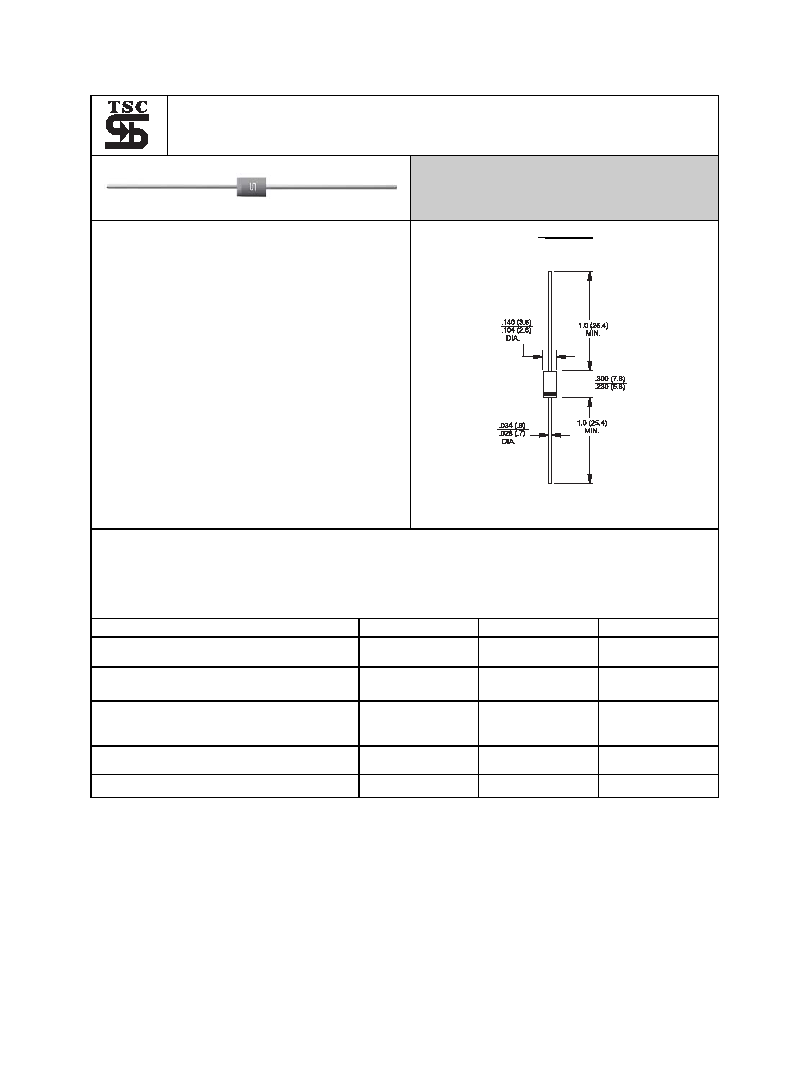
Mechanical Data
Case: Molded plastic
Lead: Axial leads, solderable per MIL-STD-
Lead:
202, Method 208
Polarity: Color band denotes cathode except
bipolar
Weight: 0.34 gram
DO-15
Dimensions in inches and (millimeters)
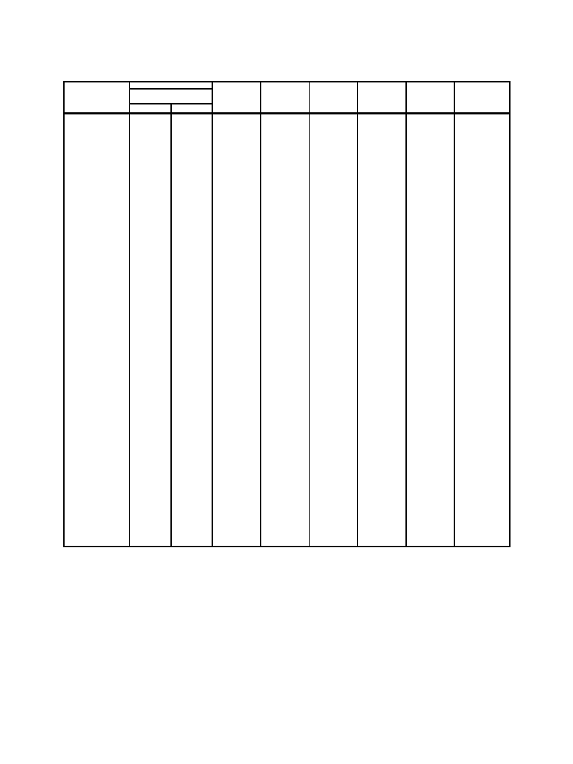
Maximum Ratings and Electrical Characteristics
Rating at 25∞C
ambient temperature unless otherwise specified.
Type Number
Symbol
Value
Units
Peak Power Dissipation at T
A
=25
O
C, Tp=1ms
(Note 1)
P
PK
Minimum
500
Watts
Steady State Power Dissipation at T
L
=75
∞C
Lead Lengths .375", 9.5mm (Note 2)
P
D
1.0
Watts
Peak Forward Surge Current, 8.3 ms Single Half
Sine-wave Superimposed on Rated Load
(JEDEC method) (Note 3)
I
FSM
70 Amps
Maximum Instantaneous Forward Voltage at
35.0A for Unidirectional Only
V
F
3.5
Volts
Operating and Storage Temperature Range
T
J
, T
STG
-55 to + 175
∞C
Notes: 1. Non-repetitive Current Pulse Per Fig. 3 and Derated above T
A
=25
O
C Per Fig. 2.
Notes:
2. Mounted on Copper Pad Area of 1.6 x 1.6" (40 x 40 mm) Per Fig. 5.
Notes:
3. 8.3ms Single Half Sine-wave or Equivalent Square Wave, Duty Cycle=4 Pulses Per Minutes
Notes:
3.
Maximum.
Devices for Bipolar Applications
Notes:
1. For Bidirectional Use C or CA Suffix for Types SA5.0 through Types SA170.
Notes:
2. Electrical Characteristics Apply in Both Directions.

- 633 -
RATINGS AND CHARACTERISTIC CURVES (SA SERIES)
FIG.2- PULSE DERATING CURVE
PEAK
PULSE
POWER
(Ppp)
or
CURRENT
()
DERA
TING
IN
PERCENT
AGE,
%
IPPM
0
25
50
75
100
125
150
175
200
0
25
50
75
100
T
AMBIENT TEMPERATURE, C
A,
o
FIG.4- MAXIMUM NON-REPETITIVE FORWARD SURGE
CURRENT UNIDIRECTIONAL ONLY
l
,
PEAK
FOR
W
ARD
SURGE
CURRENT
,
AMPERES
FSM
1
10
100
10
200
100
NUMBER OF CYCLES AT 60Hz
8.3ms Single Half Sine Wave
JEDEC Method
FIG.3- PULSE WAVEFORM
PEAK
PULSE
CURRENT
-%
0
0
1.0
2.0
3.0
4.0
100
50
t, TIME, ms
PULSE WIDTH (td) is DEFINED
as the POINT WHERE the PEAK
CURRENT DECAYS
to 50% of l
PPM
td
tr=10 sec.
m
10/1000 sec. WAVEFORM
as DEFINED by R.E.A.
m
PEAK VALUE
l
PPM
HALF VALUE- l
PPM
2
TL, LEAD TEMPERATURE, C
o
FIG.5- STEADY STATE POWER DERATING CURVE
PM
,
STEADY
ST
A
T
E
POWER
DISSIP
A
T
ION,
W
A
TTS
(A
V)
0
25
50
75
100
125
150
175
200
0
0.8
0.6
0.4
0.2
1.6
1.4
1.2
1.0
1.6 X 1.6 X .040"
(40 X 40 X 1mm.)
COPPER HEAT SINKS
L=0.375"(9.5mm)
LEAD LENGTHS
FIG.1- PEAK PULSE POWER RATING CURVE
P
,
PEAK
PULSE
POWER,
KW
PPM
0.1
ms
100ms
1,000ms
10,000ms
10ms
1ms
0.1
40
10
1
tp, PULSE WIDTH, sec.
NON-REPETITIVE
PULSE WAVEFORM
SHOWN in FIG.3
T =25 C
A
0
IMPULSE
EXPONENTIAL
DECAY
HALF SINE
SQUARE
CURRENT WAVEFORM
ld
ld
P
PK
P
PK
P
PK
5
O
ld
ld=7lp
150
- 635 -
ELECTRICAL CHARACTERISTICS (TA=25
O
C unless otherwise noted)
Breakdown Voltage
Test
Stand-Off
Maximum
Maximum
Maximum
Maximum
Device
V
BR
Current
Voltage
Reverse Leakage
Peak Pulse
Clamping
Temperature
(Volts) (Note 1)
@I
T
V
WM
at V
WM
Current I
PPM
Voltage at I
PPM
Coefficient
Min
Max
(mA)
(Volts)
I
D
(uA)
(Note 2)(Amps)
V
C
(Volts)
of V
BR
mV /
O
C)
SA45
50.0
61.1
1.0
45.0
1.0
6.5
80.3
58.0
SA45A
50.0
55.3
1.0
45.0
1.0
7.2
72.7
52.0
SA48
53.3
65.2
1.0
48.0
1.0
6.1
85.5
63.0
SA48A
53.3
58.9
1.0
48.0
1.0
6.7
77.4
56.0
SA51
56.7
69.3
1.0
51.0
1.0
5.7
91.1
66.0
SA51A
56.7
62.7
1.0
51.0
1.0
6.3
82.4
61.0
SA54
60.0
73.3
1.0
54.0
1.0
5.4
96.3
71.0
SA54A
60.0
66.3
1.0
54.0
1.0
6.0
87.1
65.0
SA58
64.4
78.7
1.0
58.0
1.0
5.0
103
78.0
SA58A
64.4
71.2
1.0
58.0
1.0
5.6
93.6
70.0
SA60
66.7
81.5
1.0
60.0
1.0
4.9
107
80.0
SA60A
66.7
73.7
1.0
60.0
1.0
5.4
96.8
71.0
SA64
71.1
86.9
1.0
64.0
1.0
4.6
114
86.0
SA64A
71.1
78.6
1.0
64.0
1.0
5.0
103
76.0
SA70
77.8
95.1
1.0
70.0
1.0
4.2
125
94.0
SA70A
77.8
86
1.0
70.0
1.0
4.6
113
85.0
SA75
88.3
102
1.0
75.0
1.0
3.9
134
101
SA75A
88.3
92.1
1.0
75.0
1.0
4.3
121
91
SA78
86.7
103
1.0
78.0
1.0
3.7
139
105
SA78A
86.7
95.8
1.0
78.0
1.0
4.1
126
95
SA85
94.4
115
1.0
85.0
1.0
3.4
151
114
SA85A
94.4
104
1.0
85.0
1.0
3.8
137
103
SA90
100
122
1.0
90.0
1.0
3.2
160
121
SA90A
100
111
1.0
90.0
1.0
3.5
146
110
SA100
111
136
1.0
100
1.0
2.9
179
135
SA100A
111
123
1.0
100
1.0
3.2
162
123
SA110
122
149
1.0
110
1.0
2.6
196
148
SA110A
122
135
1.0
110
1.0
2.9
177
133
SA120
133
163
1.0
120
1.0
2.4
214
162
SA120A
133
147
1.0
120
1.0
2.7
193
146
SA130
144
176
1.0
130
1.0
2.2
230
175
SA130A
144
159
1.0
130
1.0
2.5
209
158
SA150
167
204
1.0
150
1.0
1.9
268
203
SA150A
167
185
1.0
150
1.0
2.1
243
184
SA160
178
218
1.0
160
1.0
2.0
257
217
SA160A
178
197
1.0
160
1.0
2.0
259
196
SA170
189
231
1.0
170
1.0
1.7
304
230
SA170A
189
209
1.0
170
1.0
1.9
275
208
Notes:
1. V
BR
measured after I
T
applied for 300us, I
T
= square wave pulse or equivallent.
2. Surge current waveform per Figure 3 and derate per Figure 2.
3. For bipolar types with V
WM
of 10 Volts and under, the I
D
limit is doubled.
4. All terms and symbols are consistent ANSI/IEEE C62.35.
- 636 -
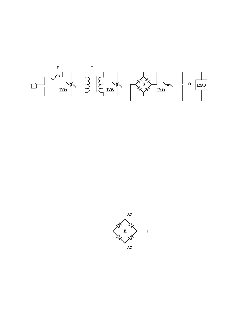
TVS APPLICATION NOTES:
Transient Voltage Suppressors may be used at various points in a circuit to provide various degrees of
protection. The following is a typical linear power supply with transient voltage suppressor units placed at
different points. All provide protection of the load.
FIGURE 1
Transient Voltage Suppressors 1 provides maximum protection. However, the system will probably require
replacement of the line fuse(F) since it provides a dominant portion of the series impedance when a surge is
encountered.
However, we do not recommend to use the TVS diode here, unless we can know the electric circuit
impedance and the magnitude of surge rushed into the circuit. Otherwise the TVS diode is easy to be
destroyed by voltage surge.
Transient Voltage Suppressor 2 provides execllent protection of circuitry excluding the transformer(T).
However, since the transformer is a large part of the series impedance, the chance of the line fuse opening
during the surge condition is reduced.
Transient Voltage Suppressor 3 provides the load with complete protection. It uses a unidirectional
Transient Voltage Suppressor, which is a cost advantage. The series impedance now includes the line fuse,
transformer, and bridge rectifier(B) so failure of the line fuse is further reduced. If only Transient Voltage
Suppressor 3 is in use, then the bridge rectifier is unprotected and would require a higher voltage and current
rating to prevent failure by transients.
Any combination of these three, or any one of these applications, will prevent damage to the load. This would
require varying trade-offs in power supply protection versus maintenance(changing the time fuse).
An additional method is to utilize the Transient Voltage Suppressor units as a controlled avalanche bridge.
This reduces the parts count and incorporates the protection within the bridge rectifier.
FIGURE 2