- 122 -
1
2
3
SRAS890 THRU SRAS8100
8.0 AMPS. Schottky Barrier Rectifiers
Voltage Range
90 to 100 Volts
Current
8.0 Amperes
Features
Low forward voltage drop
High current capability
High
reliability
High surge current capability
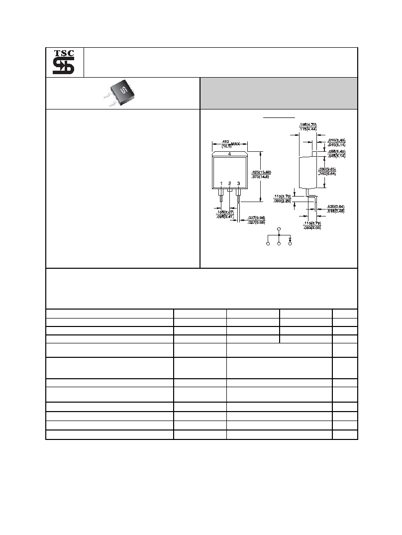
Mechanical Data
Cases: D2PAK molded plastic
Epoxy: UL 94V-O rate flame retardant
Terminals: Leads solderable per
MIL-STD-202, Method 208 guaranteed
Polarity:
As
marked
High temperature soldering guaranteed:
260
O
C/10 seconds/.25",(6.35mm) from
case
Weight: 2.24 grams
D
2
PAK
Dimensions in inches and (millimeters)
Maximum Ratings and Electrical Characteristics
Rating at 25
ambient temperature unless otherwise specified.
Single phase, half wave, 60 Hz, resistive or inductive load.
For capacitive load, derate current by 20%
Type Number
Symbol
SRAS890 SRAS8100
Units
Maximum Recurrent Peak Reverse Voltage
V
RRM
90 100
V
Maximum RMS Voltage
V
RMS
63 70
V
Maximum DC Blocking Voltage
V
DC
90 100
V
Maximum Average Forward Rectified Current
See Fig. 1
I
(AV)
8.0
A
Peak Forward Surge Current, 8.3 ms Single
Half Sine-wave Superimposed on Rated Load
(JEDEC method )
I
FSM
150
A
M
aximum
I
nstantaneous
F
orward
V
oltage
@8.0A
V
F
0.95
V
Maximum D.C. Reverse Current @ Tc=25
at Rated DC Blocking Voltage
I
R
0.1
mA
Typical Thermal Resistance (Note 1)
R
JC
3.0
/W
Typical Junction Capacitance (Note 2)
Cj 165
pF
Operating Junction Temperature Range
T
J
-65
to
+150
Storage Temperature Range
T
STG
-65
to
+150
Notes: 1. Thermal Resistance from Junction to Case Per Leg
2. Measured at 1MHz and Applied Reverse Voltage of 4.0V D.C.
- 123 -
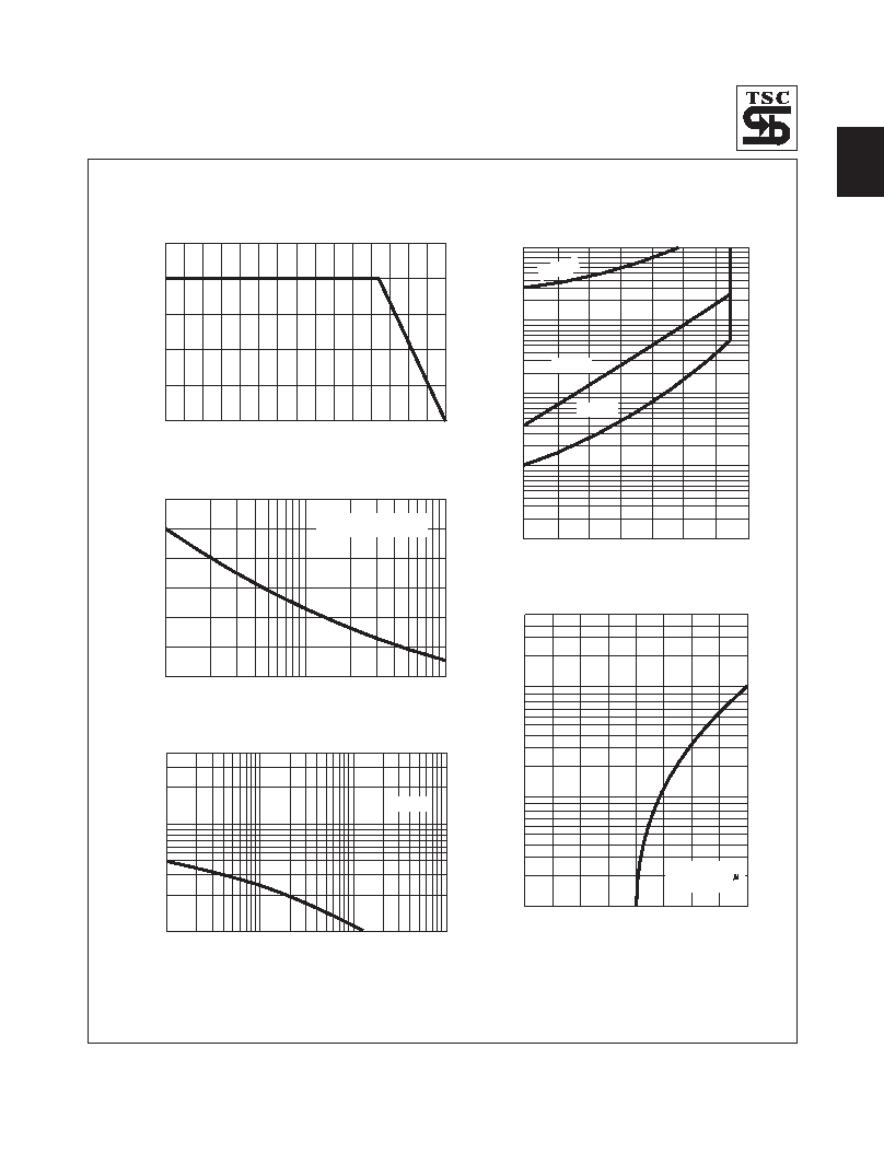
RATINGS AND CHARACTERISTIC CURVES (SRAS890 THRU
8100)
SRAS
FIG.3- MAXIMUM NON-REPETITIVE FORWARD
SURGE CURRENT
PEAK
FOR
W
ARD
SURGE
CURRENT
.
(A)
1
2
5
10
20
100
50
25
50
125
100
150
175
NUMBER OF CYCLES AT 60Hz
8.3ms Single Half Sine Wave
JEDEC Method
FIG.5- TYPICAL FORWARD CHARACTERISTICS
INST
ANT
ANEOUS
FOR
W
ARD
CURRENT
.
(A)
0.1
0.2
0.3
0.4
0.5
0.6
0.7
0.8
0.9
0.1
1.0
10
50
FORWARD VOLTAGE. (V)
FIG.4- TYPICAL JUNCTION CAPACITANCE
JUNCTION
CAP
ACIT
ANCE.(pF)
.1
.4
1.0
4
10
40
100
100
200
400
600
1000
800
2000
4000
REVERSE VOLTAGE. (V)
Tj=25 C
0
FIG.1- MAXIMUM FORWARD CURRENT DERATING
CURVE
A
VERAGE
FOR
W
ARD
CURRENT
.
(A)
0
50
100
150
0
2
4
6
8
10
CASE TEMPERATURE. ( C)
o
FIG.2- TYPICAL REVERSE CHARACTERISTICS
INST
ANT
ANEOUS
REVERSE
CURRENT
.
(mA)
20
40
60
80
100
120
.001
.01
.10
1.0
10
PERCENT OF RATED PEAK REVERSE VOLTAGE. (%)
Tj=1
25 C
0
Tj=25 C
0
Tj=75 C
0
Tj=25 C
Pulse Width=300 s
1% Duty Cycle
o
0
140