- 62 -
SSL32 THRU SSL34
3.0 AMPS. Surface Mount Low V
F
Schottky Barrier Rectifiers
Voltage Range
20 to 40 Volts
Current
3.0 Amperes
Features
For surface mounted application
Metal silicon junction, majority carrier conduction
Low
forward
voltage
drop
Easy pick and place
High surge current capability
Plastic
material
used carries Underwriters
Laboratory Classification 94V-O
Epitaxial
construction
High temperature soldering:
260
o
C / 10 seconds at terminals
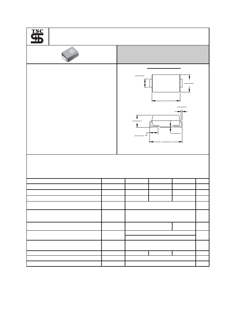
Mechanical Data
Cases: Molded plastic
Terminals: Solder plated
Polarity: Indicated by cathode band
Packaging: 16mm tape per EIA STD RS-481
Weight:
0.21gram
SMC/DO-214AB
Dimensions in inches and (millimeters)
Maximum Ratings and Electrical Characteristics
Rating at 25
ambient temperature unless otherwise specified.
Single phase, half wave, 60 Hz, resistive or inductive load.
For capacitive load, derate current by 20%
Type Number
Symbol
SSL32 SSL33 SSL34
Units
Maximum Recurrent Peak Reverse Voltage
V
RRM
20 30 40
V
Maximum RMS Voltage
V
RMS
14 21 28
V
Maximum DC Blocking Voltage
V
DC
20 30 40
V
Maximum Average Forward Rectified Current
See Fig. 1
I
(AV)
3.0 A
Peak Forward Surge Current, 8.3 ms Single
Half Sine-wave Superimposed on Rated Load
(JEDEC method )
I
FSM
100 A
Maximum Instantaneous Forward Voltage
(Note 1) @3.0A
V
F
0.385 0.40
V
1.0
Maximum DC Reverse Current @ T
A
=25
at
Rated DC Blocking Voltage @ T
A
=100
I
R
150
mA
mA
Maximum Thermal Resistance (Note 2)
R
JL
R
JA
17
55
/W
Marking Code
SL32
SL33
SL34
Operating Temperature Range
T
J
-55
to
+125
Storage Temperature Range
T
STG
-55
to
+
150
Notes:1. Pulse Test with PW=300 usec, 1% Duty Cycle.
2. Measured on P.C. Board with 0.6 x 0.6"(16 x 16mm) Copper Pad Areas.
.129(3.27)
.118(3.0)
.012(.31)
.006(.15)
.008(.20)
.004(.10)
.060(1.52)
.030(0.76)
.245(6.22)
.220(5.59)
.280(7.11)
.260(6.60)
.103(2.62)
.079(2.00)
.320(8.13)
.305(7.75)
- 63 -
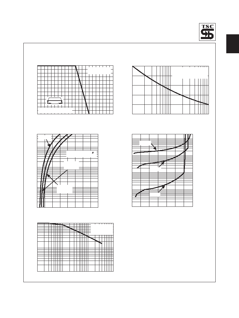
RATINGS AND CHARACTERISTIC CURVES (SSL32 THRU SSL34)
FIG.4- TYPICAL REVERSE CHARACTERISTICS
INST
ANT
ANEOUS
REVERSE
CURRENT
.
(mA)
0
20
40
60
80
100
120
140
0.001
0.01
0.1
1
10
20
PERCENT OF RATED PEAK REVERSE VOLTAGE. (%)
TJ=25 C
0
TJ=100 C
0
TJ=75 C
0
FIG.2- MAXIMUM NON-REPETITIVE PEAK FORWARD
SURGE CURRENT
PEAK
FOR
W
ARD
SURGE
CURRENT
.
(A)
1
10
100
0
20
40
80
60
100
NUMBER OF CYCLES AT 60Hz
AT RATED TL
8.3ms Single Half Sine Wave
JEDEC Method
FIG.3- TYPICAL FORWARD CHARACTERISTICS
INST
ANT
ANEOUS
FOR
W
ARD
CURRENT
.
(A)
0
0.2
0.4
0.6
0.8
1.0
1.2
1.4
1.6
0.01
0.1
1
10
50
FORWARD VOLTAGE. (V)
Tj=125 C
0
Tj=25 C
0
FIG.5- TYPICAL JUNCTION CAPACITANCE
JUNCTION
CAP
ACIT
ANCE.(pF)
0.1
1
10
100
10
100
1000
REVERSE VOLTAGE. (V)
Tj=25 C
f=1.0MHz
Vsig=50mVp-p
0
FIG.1- MAXIMUM FORWARD CURRENT DERATING
CURVE
A
VERAGE
FOR
W
ARD
CURRENT
.
(A)
50
60
70
80
90
100
110
120
160
150
140
130
0
1
2
3
LEAD TEMPERATURE. ( C)
o
RESISTIVE OR
INDUCTIVE LOAD
PCB MOUNTED ON 0.6X0.6"
(16X16mm) COPPER PAD AREAS
PULSE WIDTH=300 S
1% DUTY CYCLE
SSL32-33
Tj=25 C
0
SSL34