
- 852 -
TAR3525
35.0 AMPS. Load Dump Rectifiers
Voltage Range
24 to 32 Volts
Current
35.0 Amperes
Features
Plastic material used carries Underwriters
Laboratory Classification 94V-O
Low cost construction utilizing void-free molded
plastic technique
Low
cost
Diffused
junction
Low
leakage
High
surge
capability
High temperature soldering guaranteed:
260
o
C for 10 seconds
Mechanical Data
Case: Molded plastic case
Terminals: Plated terminals, solderable per MIL-
STD-202, Method 208
Polarity: Color ring denotes cathode end
Weight: 0.07 ounce, 1.8 grams
Mounting position: Any
AR
Dimensions in inches and (millimeters)
Maximum Ratings and Electrical Characteristics
Rating at 25
ambient temperature unless otherwise specified.
Single phase, half wave, 60 Hz, resistive or inductive load.
For capacitive load, derate current by 20%
Type Number
Symbol
TAR3525 Units
Maximum Recurrent Peak Revere Voltage
V
RRM
Working Peak Reverse Voltage
V
RMS
Maximum DC Blocking Voltage
V
DC
20 V
Reverse Zener Voltage (Note 1)
V
Z
24 Min
32 Max
V
Maximum Clamping Voltage VC (Note 2)
V
C
35 V
Maximum Average Forward Rectified Current
@ Tc = 100
I
F
35
A
Non-Repetitive Peak Forward Surge Current,
(half wave, single phase, 60 Hz sine applied to
rated load)
I
FSM
600 A
Repetitive Peak Reverse Surge Current (Time
Constant = 10 mSec Duty Cycle <1.0%, TC=25
I
RSM
110 A
MaximumInstantaneous Forward Voltage
(IF=100A @ 400uSec pulse, Tc=25
)
V
F
1.1
V
Maximum DC Reverse Current (at Rated DC
Blocking Voltage @Tc=25
)
I
R
200
nA
Maximum Thermal Resistance, Junction to
Case (Note 3)
R
JC
0.8
/W
O
perating
and
Storage Temperature Range
T
J
, T
STG
-50 to +175
Notes: 1. Reverse Zener Voltage Test Conditions: IR=5mA, TC=25
, PW=30mS
.
2. VC Test Conditions: IR=65A, TC=25
, PW=100uS.
3. Single Side Cooled.
- 853 -
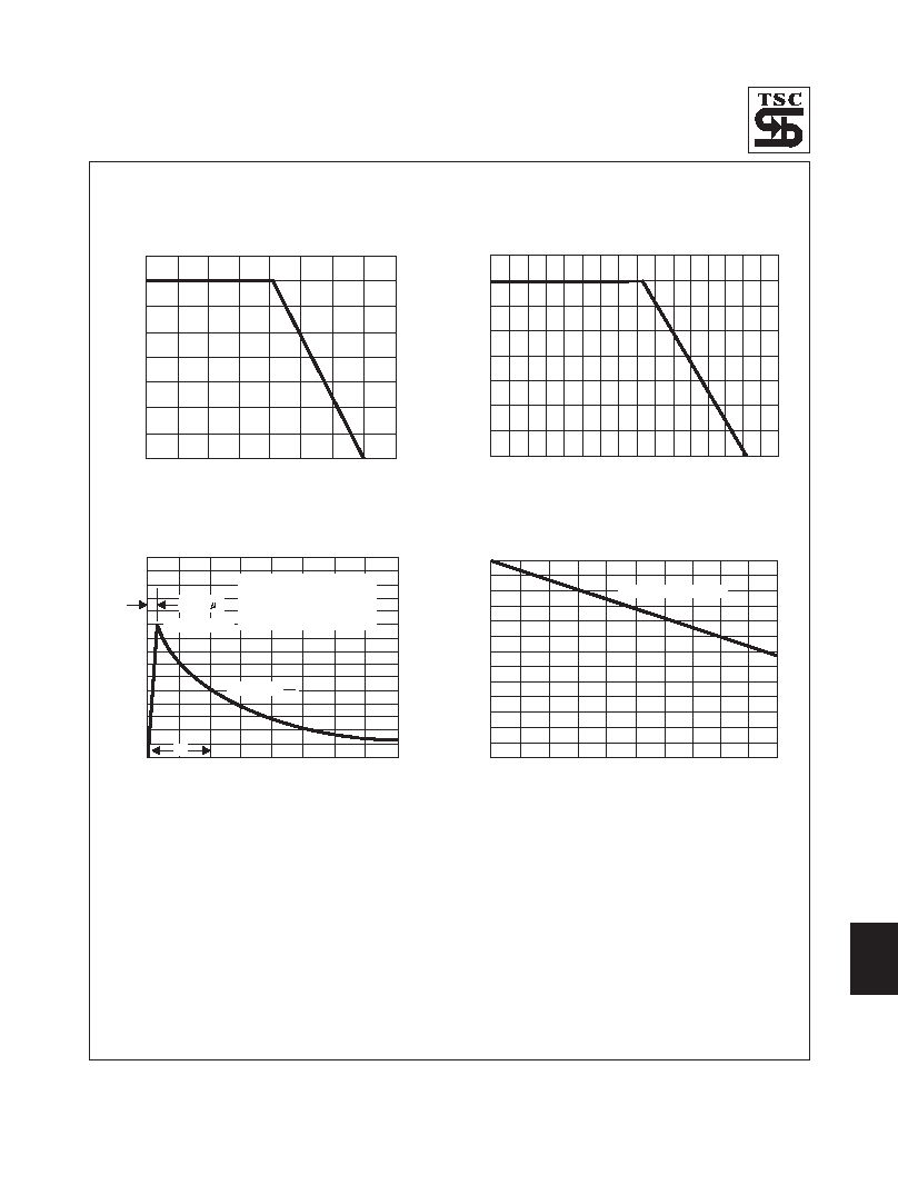
RATINGS AND CHARACTERISTIC CURVES (TAR3525)
POWER
DISSIP
A
TION
(W)
CASE TEMPERATURE ( C)
O
0
50
100
150
200
0
10
20
30
40
FIG.1- POWER DERATING CURVE
FIG.2- MAXIMUM FORWARD CURRENT DERATING
CURVES
IF
,
A
VERAGE
FOR
W
ARD
CURRENT
(A)
TC, CASE TEMPERATURE ( C)
O
0
25
50
75
100
125
150
175
200
0
10
20
30
40
FIG.3- PULSE WAVEFORM
FIG.4- REVERSE POWER DERATING
INPUT
PEAK
PULSE
CURRENT
%
TIME, ms (t)
0
10
20
30
40
0
50
100
150
tr = 10 s
Peak Value I
PP
Half Value - I
PP
2
T = 25 C
Pulse width (td) is defined as
the point where the peak
current decays to 50% of I
J
O
PP
td
PRSM,
PEAK
REVERSE
POWER
(W)
TC, CASE TEMPERATURE ( C)
O
25
50
75
100
125
150
1200
1600
2000
2400
2800
3200
3600
3800
Time Constant = 10 ms