
TS1086
1-1
2003/12 rev. B
TS1086
1.5A Low Dropout Positive Voltage Regulator
Low Dropout Voltage 1.3V max.
General Description
The TS1086 Series are high performance positive voltage regulators are designed for use in applications requiring low
dropout performance at full rated current, Additionally, the PJ1086 Series provides excellent regulation over variations due
to changes in line, load and temperature. Outstanding features include low dropout performance at rated current, fast
transient response, internal current limiting and thermal shutdown protection of the output device. The TS1086 Series are
three terminal regulators with fixed and adjustable voltage options available in popular packages.
This series is offered in 3-pin TO-263, TO-220, TO-252 and SOT-223 package.
Features
Low dropout performance 1.3V max.
Full current rating over line and temperature.
Fast transient response
±
2%Total output regulation over line, load and
temperature
Adjust pin current max 90A over temperature
Line regulation typical 0.015%.
Load regulation typical 0.05%.
Fixed/adjustable output voltage
TO-220, TO-263 TO-252 and SOT-223 package
Block Diagram
Ordering Information
Part No.
Operating Temp.
(Ambient)
Package
TS1086CZ
xx
TO-220
TS1086CM
xx
TO-263
TS1086CP
xx
TO-252
TS1086CW
xx
-20 ~ +85
o
C
SOT-223
Note: Where
xx
denotes voltage option, available are
5.0V, 3.3V, 2.5V and 1.8V. Leave blank for
adjustable version. Contact factory for additional
voltage options.
Absolute Maximum Rating
Input Supply Voltage
Vin
12
V
Operation Input Supply Voltage Vin
(operate)
7
V
Power Dissipation
P
D
Internally Limited
W
Operating Junction Temperature Range
T
J
-25 ~ +150
o
C
Storage Temperature Range
T
STG
-65 ~ +150
o
C
Lead Soldering Temperature (260
o
C)
TO-220 / TO-263 Package
TO-252 / SOT-223 Package
10
5
S
TO-263
Pin assignment:
1. Ground / Adj
2. Output
3. Input
Pin 2 connect to heatsink

TS1086
2-2
2003/12 rev. B
Electrical Characteristics
Ta = 25
o
C, unless otherwise specified. Adjustable version test with Vout = 2.5V.
Parameter Conditions
Min
Typ
Max
Unit
Vout+1.5V
Vin 7V, Io=10mA
0.990|Vo|
1.010|Vo|
V
Output Voltage
Vout+1.5V
Vin 7V, Io=1.5A
0.980|Vo|
5.0 / 3.3
2.5 / 1.8
1.020|Vo| V
(Vin-out) =1.5V, Io=10mA
0.990|Vo|
1.010|Vo|
V
Reference Voltage
(Vin-out) =1.5V, Io=1.5A
0.980|Vo|
1.25
1.020|Vo| V
Input Supply Voltage
--
--
7
V
Line Regulation
Vout+1.5V
Vin 7V, Io=10mA
--
0.015
0.2
%
%
Load Regulation (note 1,2) Vin=Vout+1.5V,
10mA
Io
1.5A
-- 0.05 1.0
%
Dropout Voltage
Io=1.5A, Vout=0.1%Vout --
1.3
1.4
V
Minimum Load Current
Vin=5V
--
8
10
mA
Adjustable Pin Current
--
90
--
uA
Current Limit
Vin - Vout=3V
2.0
--
--
A
Temperature Stability
Io=10mA
-- 0.5 -- %
Ripple Rejection
F = 120Hz, Io=1.5A Cout=25uF,
Vin=Vout + 3V
-- 60 70
dB
Thermal Performance
Condition Package
type
Typ Unit
TO-220 45
TO-263 45
TO-252 80
Thermal Resistance
Junction to Ambient
SOT-223 100
o
C/W
Note 1: See thermal regulation specification for changes in output voltage due to heating effects. Line and load regulation
are measured at a constant junction temperature by low duty cycle pulse testing. Load regulation is measured at
the output lead = 1/18" from the package.
Note 2: Line and load regulation are guaranteed up to the maximum power dissipation of 15W. Power dissipation is
determined by the input / output voltage difference and the output current. Guaranteed maximum power
dissipation will not be available over the full input / output voltage range.
Note 3: Quiescent current is defined as the minimum output current required to maintain the regulation.
TS1086
3-3
2003/12 rev. B
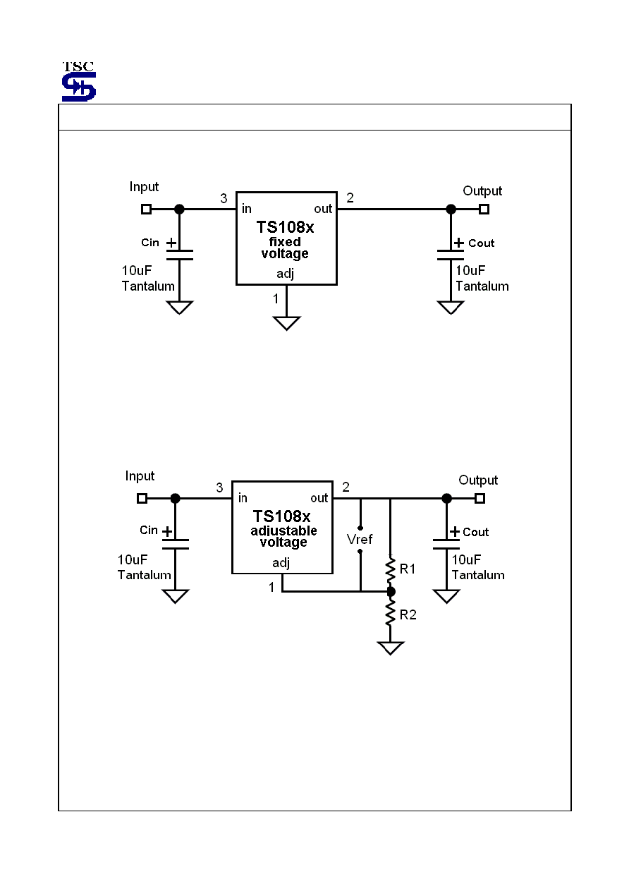
Typical Application Circuit
Fixed output voltage version
Vout = Vref * (1 + R2 / R1)
*
Cin is requested if regulator is located
Far from power supply filter
**
Design Cout as close to Vout pin as possible
Adjustable output voltage version
TS1086
4-4
2003/12 rev. B
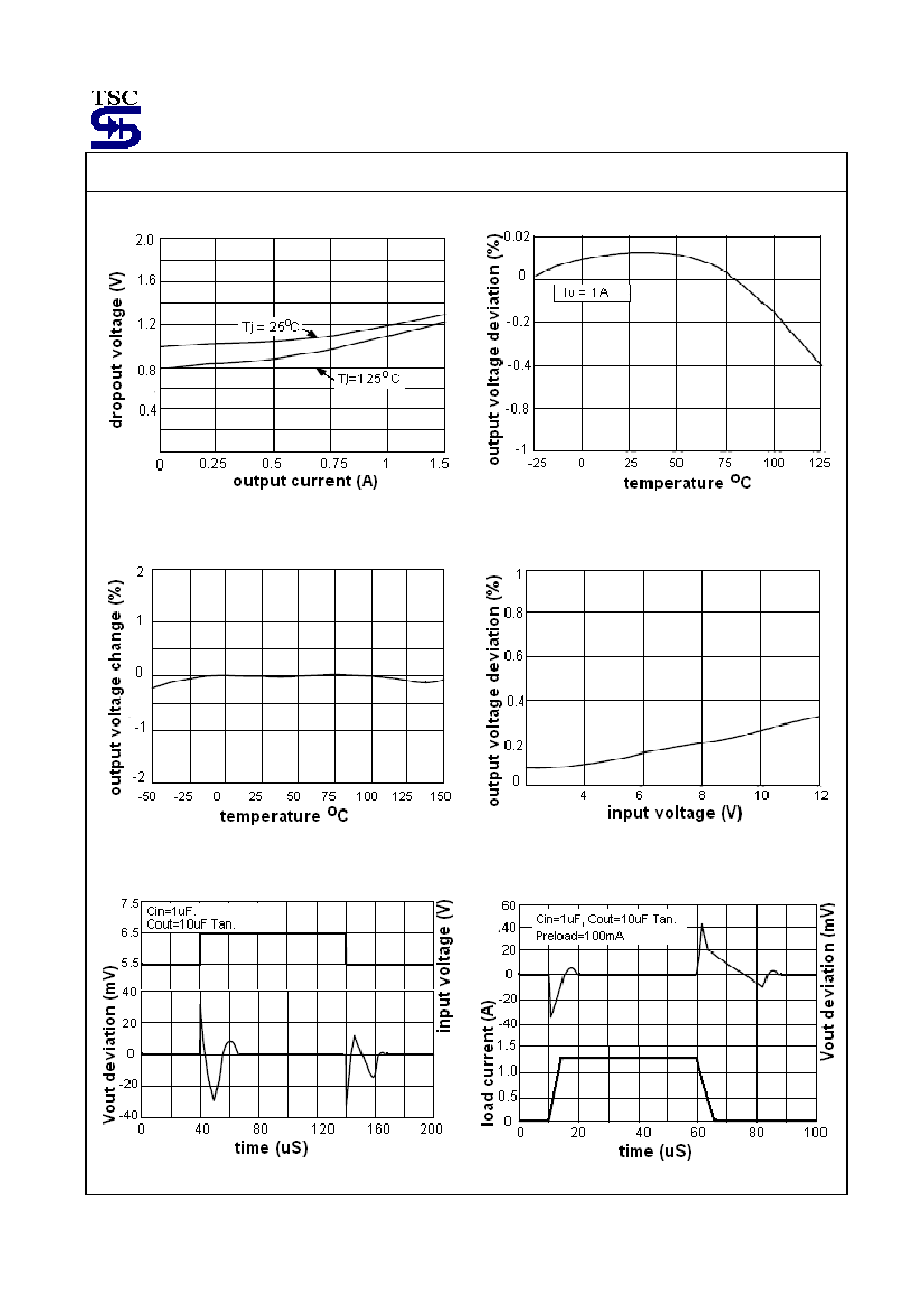
Electrical Characteristics Curve
Figure 1: dropout voltage v.s. output current
Figure 2: load regulation v.s. temp.
Figure 3: output change v.s. temp.
Figure 4: line regulation
Figure 5: line transient response
Figure 6: load transient response

TS1086
5-5
2003/12 rev. B
TO-220 Mechanical Drawing
I
J
H
E
G
F
D
C
B
A
M
N
O
L
K
P
TO-220 DIMENSION
MILLIMETERS INCHES
DIM
MIN MAX MIN MAX
A 10.000 10.500 0.394 0.413
B 3.240 4.440 0.128 0.175
C 2.440 2.940 0.096 0.116
D - 6.350 - 0.250
E 0.381 1.106 0.015 0.040
F 2.345 2.715 0.092 0.058
G 4.690 5.430 0.092 0.107
H 12.700 14.732 0.500 0.581
I 8.382 9.017 0.330 0.355
J 14.224 16.510 0.560 0.650
K 3.556 4.826 0.140 0.190
L 0.508 1.397 0.020 0.055
M 27.700 29.620 1.060 1.230
N 2.032 2.921 0.080 0.115
O 0.255 0.610 0.010 0.024
P 5.842 6.858 0.230 0.270
TO-263 Mechanical Drawing
A
D
B
C
H
G
E
F
I
TO-263 DIMENSION
MILLIMETERS INCHES
DIM
MIN MAX MIN MAX
A 10.000 10.500 0.394 0.413
B 14.605 15.875 0.575 0.625
C 0.508 0.991 0.020 0.039
D 2.420 2.660 0.095 0.105
E 4.064 4.830 0.160 0.190
F 1.118 1.400 0.045 0.055
G 0.450 0.730 0.018 0.029
H 8.280 8.800 0.325 0.346
I 1.140 1.400 0.044 0.055
J 1.480 1.520 0.058 0.060

TS1086
6-6
2003/12 rev. B
TO-252 Mechanical Drawing
B
C
D
A
F
G
I
H
E
J
TO-252 DIMENSION
MILLIMETERS INCHES
DIM
MIN MAX MIN MAX
A 6.570 6.840 0.259 0.269
B 9.250 10.400 0.364 0.409
C 0.550 0.700 0.022 0.028
D 2.560 2.670 0.101 0.105
E 2.300 2.390 0.090 0.094
F 0.490 0.570 0.019 0.022
G 1.460 1.580 0.057 0.062
H 0.520 0.570 0.020 0.022
I 5.340 5.550 0.210 0.219
J 1.460 1.640 0.057 0.065
SOT-223 Mechanical Drawing
G
H
E
D
F
C
A
B
J
K
I
SOT-223 DIMENSION
MILLIMETERS INCHES
DIM
MIN MAX MIN MAX
A 6.350 6.850 0.250 0.270
B 2.900 3.100 0.114 0.122
C 3.450 3.750 0.136 0.148
D 0.595 0.635 0.023 0.025
E 4.550 4.650 0.179 0.183
F 2.250 2.350 0.088 0.093
G 0.835 1.035 0.032 0.041
H 6.700 7.300 0.263 0.287
I 0.250 0.355 0.010 0.014
J 10∞ 16∞ 10∞ 16∞
K 1.550 1.800 0.061 0.071