TS1451 1-7
2003/12
rev.
A
TS1451
Dual Channel PWM Controller
Supply Voltage Range 3.6 V to 40V
Output Driving Current 20mA
Oscillator Frequency up to 500KHz
General Description
The TS1451 integrates dual channel PWM control circuit into a single chip, mainly designs for power supply regulator.
All the functions included an on-chip 2.5V reference output, two error amplifiers, and adjustable oscillator, two
dead-time comparators, under voltage lock out, short circuit protection, and dual common-emitter output transistor
circuit.
Recommend the output CE transistors as pre-driver for driving extremely. the dead time control can provide from 0% to
100%. Switching frequency can be adjustable by trimming RT and CT. During low Vcc situation, the under voltage lock
out makes sure that the output are off until the internal circuit is operational normally.
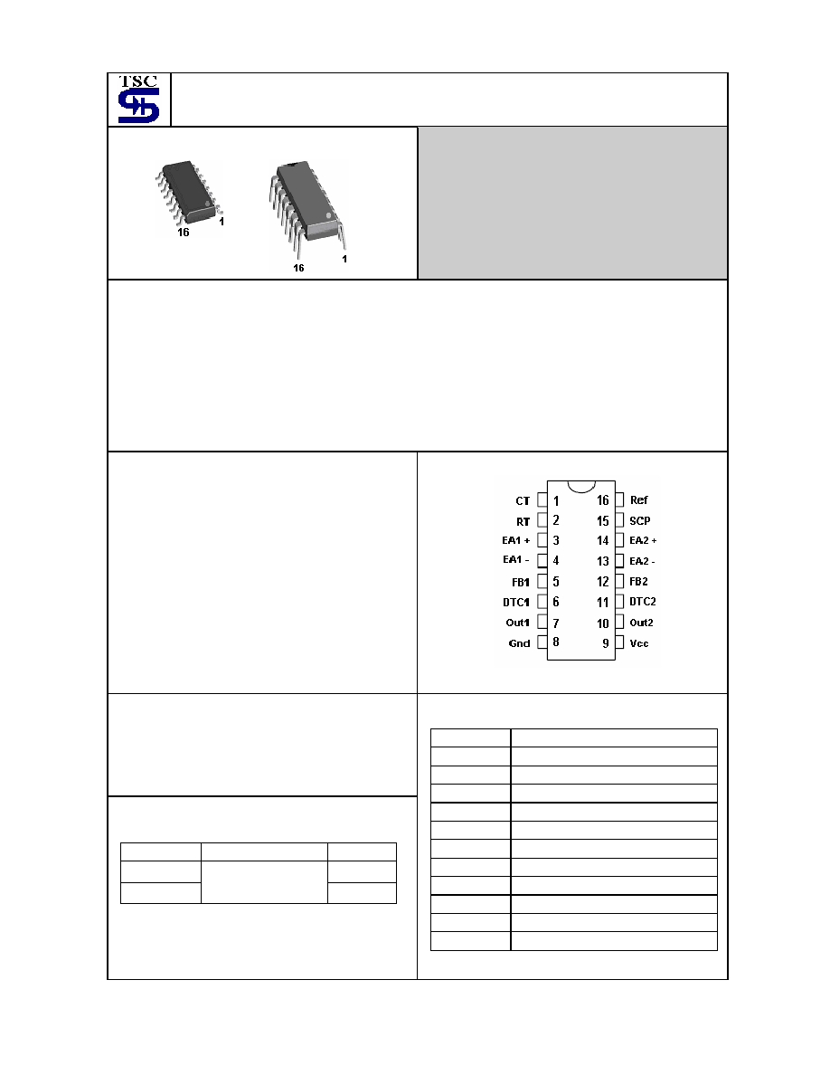
The TS1451 is offered in SOP-16 and DIP-16 package.
Features
Dual PWM Power Control Circuitry
Operating Voltage Can be up to 50V
Adjustable Dead Time Control (DTC)
Under Voltage Lock Out protection (UVLO)
Short Circuit Protection (SCP)
Variable Oscillator Frequency up to 500KHz
2.5V Voltage Reference Output
Pin Assignments
Applications
Backlight
Inverter
DC to DC Converters in Computers
Ordering Information
Part No.
Operating Temp. Package
TS1451CD DIP-16
TS1451CS
0 ~ +70
o
C
SOP-16
Pin Descriptions
Name Descriptions
CT
Timing Capacitor
RT
Timing Resistor
EA+
Error Amplifier Input (+)
EA-
Error Amplifier Input (-)
FB
Feedback Loop Compensation
DTC
Dead Time Control
Out
Pre-Driver Output
Gnd
Ground
Vcc
Supply Voltage
SCP
Short Circuit Protection
Ref
Voltage Reference
SOP-16
DIP-16
TS1451 2-7
2003/12
rev.
A
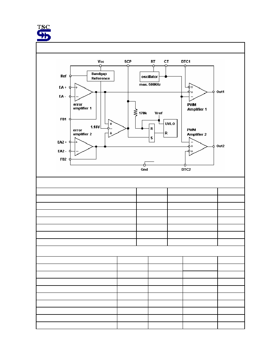
Function Block Diagram
Absolute Maximum Rating
Rating Symbol
Value
Unit
Power Supply Voltage
Vcc
40
V
Collector Output Voltage
Vo
40
V
Collector Output Current
Io
21
mA
Amplifier Input Voltage Range
Vin
20
V
Operating Junction Temperature
Tj
- 20 ~ +85
o
C
Storage Temperature Range
Tstg
-65 ~ +150
o
C
Lead Temperature 1.6mm from case for 10 sec.
Tled
260
o
C
Recommended Operating Conditions
Rating Symbol
Min.
Max
Unit
Power Supply Voltage
Vcc
3.6
40
V
Collector Output Voltage
Vo
--
40
V
Collector Output Current (each transistor)
Io
--
20
mA
Amplifier Input Voltage
Vin
1.05
1.45
V
Current Into Feedback Terminal
Ifb
--
45
uA
Feedback Resistor
Rf
100
--
K
Timing Resistor
R
T
5.1 100
K
Timing Capacitor
C
T
150 15000
pF
Oscillator Frequency
Fosc
1
500
KHz
TS1451 3-7
2003/12
rev.
A
Electrical Characteristics
(Ta= 25
o
C, V
CC
= 6V, f= 200KHz; unless otherwise specified)
REFERENCE SECTION
Parameter Test
Conditions
Min
Typ
Max
Unit
Output voltage (Vref)
Io=1mA
2.45
2.5
2.6
V
Line regulation
Vcc= 3.6V to 40V
--
2.0
12.5
Load regulation
Io= 0.1mA to 1mA
--
1.0
7.5
mV
Output voltage change with temp.
Ta=Min to Max
--
- 0.2
+/-1
%
Short-circuit output current
Vref= 0
3
10
30
mA
UNDERVOLTAGE LOCKOUT SECTION
Parameter Test
Conditions
Min
Typ
Max
Unit
Upper threshold voltage (Vcc)
--
2.65
--
V
Lower threshold voltage (Vcc)
--
2.45
--
V
Hysterics (Vcc)
Io(ref)= 0.1mA
80 200 -- mV
SHORT-CIRCUIT PROTECTION CONTROL SECTION
Parameter Test
Conditions
Min
Typ
Max
Unit
Input threshold voltage
0.65
0.7
0.75
V
Standby voltage
No pull up
140
185
--230
mV
Latched input voltage
No pull up
--
60
120
mV
Input (source) current
Vin= 0.7V
- 10
- 15
- 20
uA
Comparator threshold voltage (FB)
--
1.18
--
V
OSCILLATOR SECTION
Parameter Test
Conditions
Min
Typ
Max
Unit
Frequency C
T
= 330pF, R
T
= 10K
--
200
--
KHz
Standard deviation of frequency
C
T
= 330pF, R
T
= 10K
--
10
--
Frequency change with voltage
Vcc= 3.6V to 40V
--
1
--
Frequency change with temperature
Ta= Min to Max
--
--
+/- 2
%
DEAD-TIME CONTROL SECTION
Parameter Test
Conditions
Min
Typ
Max
Unit
Input bias current
--
--
1
Latch mode (source) current
- 80
- 145
--
uA
Latch input voltage
Io= 40uA
2.3
--
--
Zero duty cycle
--
2.05
2.25
Input threshold voltage at f= 10KHz
Maximum duty cycle
1.2
1.45
--
V
OUTPUT SECTION
Parameter Test
Conditions
Min
Typ
Max
Unit
Leakage current
Vo= 40V
--
--
10
uA
Output saturation voltage
Io= 10mA
--
1.2
2
V
Short-circuit output current
Vo= 6V
--
90
--
mA

TS1451 4-7
2003/12
rev.
A
Electrical Characteristics
(Continued)
ERROR AMPLIFIER SECTION
Parameter Test
Conditions
Min
Typ
Max
Unit
Input offset voltage
Vo(FB)= 1.25V
--
--
+/- 6
mV
Input offset current
Vo(FB)= 1.25V
--
--
+/- 100
nA
Input bias current
Vo(FB)= 1.25V
--
160
500
nA
Common-mode input voltage range
Vcc= 3.6V to 40V
1.05 to 1.45
V
Open-loop voltage amplification
Rf= 200K
70
80
--
dB
Unity-gain bandwidth
--
1.5
--
MHz
Common-mode rejection ratio
60
80
--
dB
Maximum output voltage
Vref-0.1
--
--
V
Minimum output voltage
--
--
1
V
Output sink current (FB)
V
ID
= -0.1, Vo= 1.25V
0.5
1.6
--
mA
Output source current (FB)
V
ID
= 0.1, Vo= 1.25V
-45
-70
--
uA
PWM COMPARATOR SECTION
Parameter Test
Conditions
Min
Typ
Max
Unit
Input threshold voltage (FB)
f= 10KHz
Zero duty cycle
--
2.05
2.25
V
Input sink current (pin 3)
Maximum duty cycle
1.2
1.45
--
mA
TOTAL DEVICE
Parameter Test
Conditions
Min
Typ
Max
Unit
Standby supply current
Off-state
--
2.5
3.0
Average supply current
RT= 10K
--
2.8
3.5
mA

TS1451 5-7
2003/12
rev.
A
Parameter Measurement Information
TS1451 6-7
2003/12
rev.
A
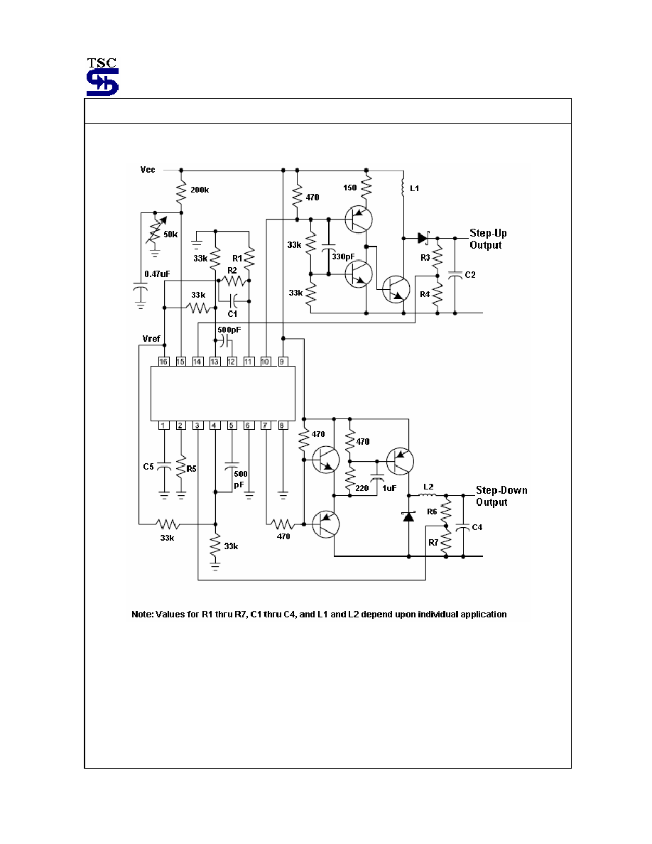
Application Information
Fig 3. High Speed Dual Switching Regulator

TS1451 7-7
2003/12
rev.
A
SOP-16 Mechanical Drawing
R
M
F
SOP-16 DIMENSION
MILLIMETERS INCHES
DIM
MIN MAX MIN MAX
A 9.80 10.00 0.386 0.393
B 3.80 4.00 0.150 0.157
C 1.35 1.75 0.054 0.068
D 0.35 0.49 0.014 0.019
F 0.40 1.25 0.016 0.049
G
1.27 (typ)
0.05 (typ)
K 0.10 0.25 0.004 0.009
M 0
o
7
o
0
o
7
o
P 5.80 6.20 0.229 0.244
R 0.25 0.50 0.010 0.019
DIP-16 Mechanical Drawing
D
G
K
C
N
A
1
16
B
8
9
L
M
J
DIP-16 DIMENSION
MILLIMETERS INCHES
DIM
MIN MAX MIN MAX
A 17.80 18.05 0.701 0.710
B 6.22 6.48 0.290 0.299
C 3.18 4.45 0.125 0.135
D 0.35 0.55 0.019 0.020
G
1.27 (typ)
0.05 (typ)
J 0.25 0.31 0.010 0.012
K 3.25 3.35 0.128 0.132
L 7.75 8.00 0.305 0.315
M - 10
o
- 10
o