TS2026
1-7
2005/11 rev. A
TS2026
Dual-Channel Power Distribution Switch
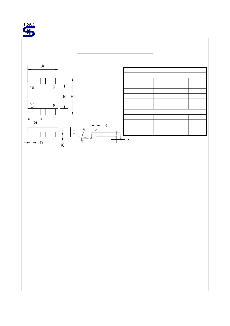
Pin assignment:
1. ENA 5. OUTB
2. FLGA 6. GND
3. FLGB 7. IN
4. ENB 8. OUTA
140m max. on-resistance per channel
2.7V to 5.5V operating range
Under voltage lockout
General Description
The TS2026 is high-side MOSFET switches optimized for general-purpose power distribution requiring circuit protection.
The TS2026 are internally current limited and have thermal shutdown that protects the device and load. When a thermal
shutdown fault occurs, the output is latched off until the faulty load is removed. Removing that load or toggling the enable
input will reset the device output. Both device employ soft-start circuitry that minimized inrush current in application
where highly capacitive loads are employed. A fault status output flag is asserted during over current and thermal
shutdown conditions. Transient faults are internally filtered.
Features
140m max. on-resistance per channel
2.7V to 5.5V operating range
500mA min. continuous current per channel
Short-circuit protection with thermal shutdown
Thermal isolated channels.
Fault status flag with 3ms filter eliminates false
assertions.
Under voltage lockout
Reverse current flow blocking (no "body diode")
Logic-compatible inputs
Soft-start circuit
Low quiescent current
Ordering Information
Part No.
Operating Temp.
(Ambient)
Package
TS2026CS
-20 ~ +85
o
C
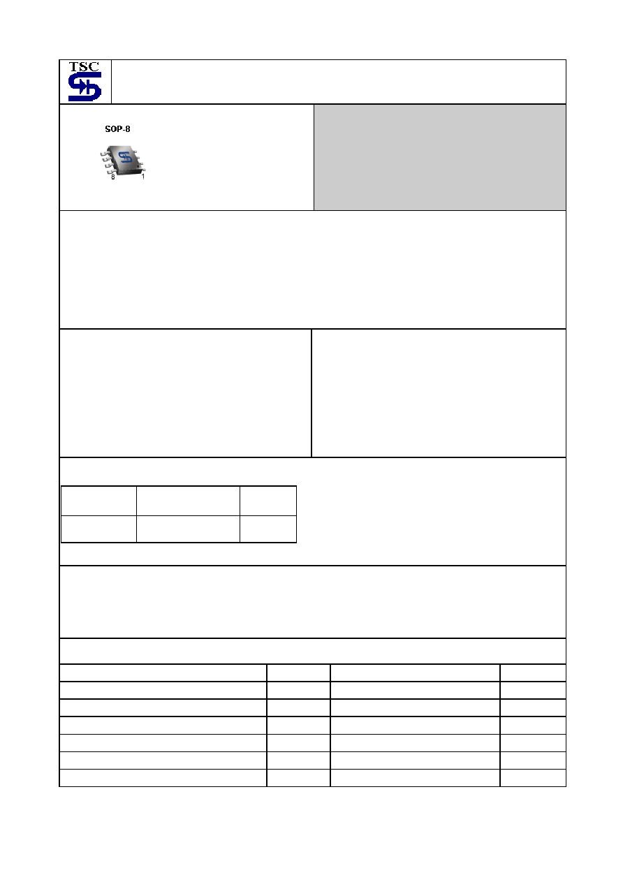
SOP-8
Applications
USB peripherals
General purpose power switching
ACPI power distribution
Notebook PCs
PDAs
PC card hot swap
Absolute Maximum Rating
Supply Voltage
V
IN
+6
V
Fault Flag Voltage
V
FLG
+6
V
Fault Flag Current
I
FLG
25
mA
Output Voltage
V
OUT
+6
o
C
Output Current
I
OUT
Internal Limited
Enable input
I
EN
-0.3 ~ +3
V
Storage Temperature
T
STG
-65 ~ +150
o
C
TS2026
2-7
2005/11 rev. A
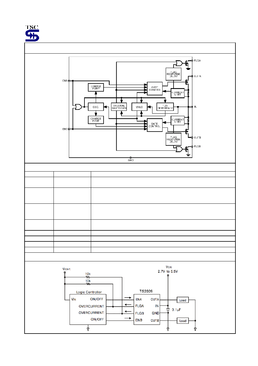
Block Diagram
Pin Description
Pin Number
Pin Name
Pin Function
1
ENA
Switch A Enable (Input): Logic-compatible enable input. Active high (H) or active
low (L)
2
FLGA
Fault Flag A (Output): Active-low, open-drain output. Indicated over current or
thermal shutdown conditions. Over current conditions mush last longer than t
D
in
order to assert FLGA
3
FLGB
Fault Flag B (Output): Active-low, open-drain output. Low Indicated over current
or thermal shutdown conditions. Over current conditions mush last longer than t
P
in order to assert FLGA
4
ENB
Switch B Enable (Input): Logic-compatible enable input. Active-high (H) or
active-low
5
OUTB
Switch B (Output)
6
GND
Ground
7
IN
Input: Switch and logic supply input
8
OUTA
Switch A (Output)
Typical Application
TS2026
3-7
2005/11 rev. A
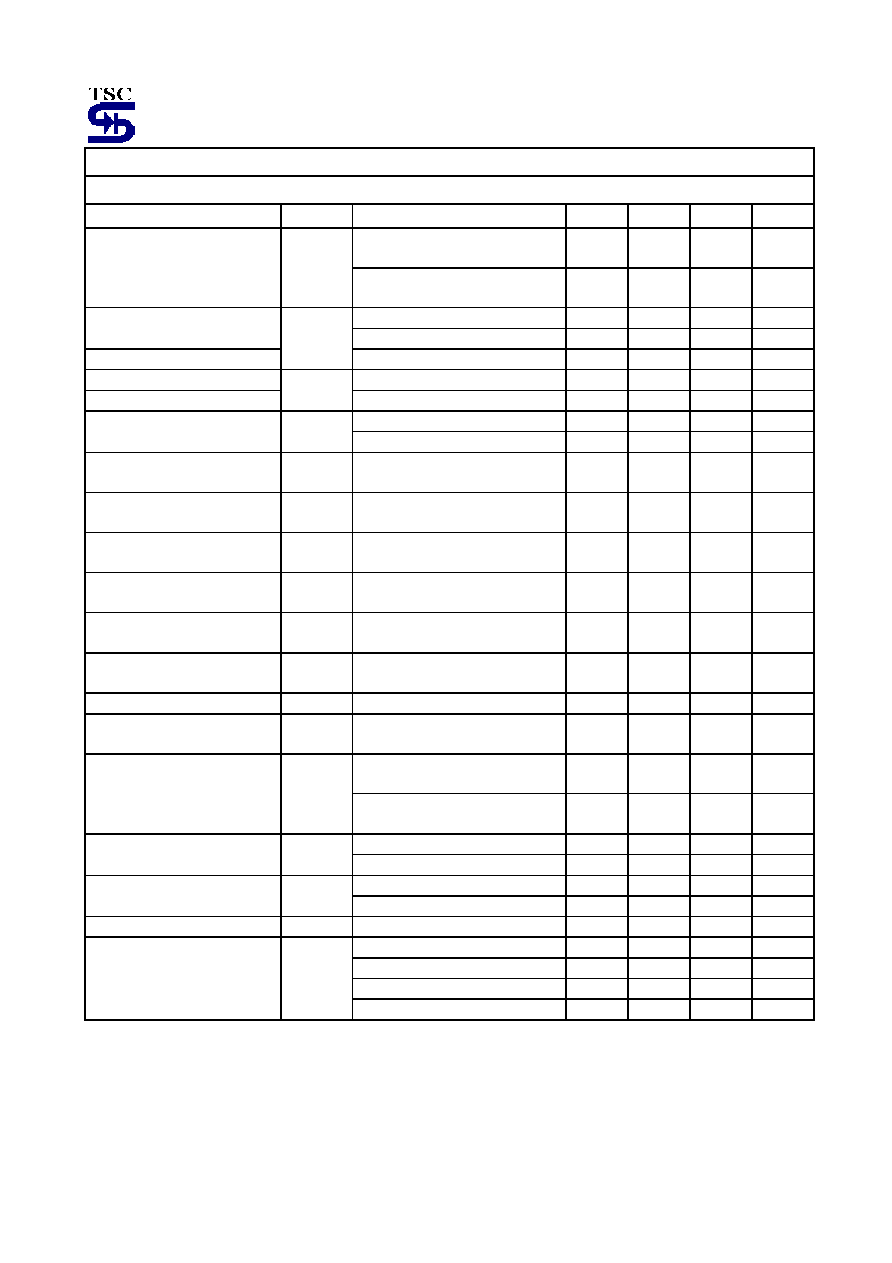
Electrical Characteristics
Vin=5V, T
A
= 25
o
C, bold values indicate -40
o
C T
A
85
o
C unless noted
Parameter
Symbol
Condition
Min.
Typ.
Max.
Units
TS2026-L, V
ENA
=V
ENB
2.4V
(switch off), OUT = open
--
0.75
5
A
Supply Current
I
DD
TS2026-H, V
ENA
=V
ENB
0.8V
(switch on), OUT = open
--
100
160
A
Low-to-high transition
--
1.7
2.4
V
Enable Input threshold
High-to-low transition
0.8
1.455
--
V
Enable Input Hysteresis
V
EN
--
250
--
mV
Enable Input Current
V
ENA
= 0V to 5.5V
-1
0.01
1
A
Enable Input Capacitance
I
EN
--
1
--
pF
V
IN
= 5V, I
OUT
= 500mA
--
90
140
m
Switch Resistance Note 4
R
DS(ON)
V
IN
= 3.3V, I
OUT
= 500mA
--
100
160
m
Output Leakage Current
TS2026-H, V
ENX
0.8V
TS2026-L, V
ENX
2.4V
--
--
10
A
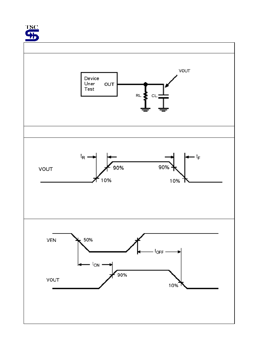
Output Turn-on Delay
t
ON
R
L
=10, C
L
=1F,
see "Timing Diagrams"
--
1.3
5
mS
Output Turn-on Rise Time
t
R
R
L
=10, C
L
=1F,
see "Timing Diagrams"
--
1.15
4.9
mS
Output Turn-off Delay
t
OFF
R
L
=10, C
L
=1F,
see "Timing Diagrams"
--
35
100
S
Output Turn-off Fall Time
t
F
R
L
=10, C
L
=1F,
see "Timing Diagrams"
--
32
100
S
Short-Circuit Output Current
I
LIMIT
V
OUT
= 0V, enable into
short-circuit
0.5
0.9
1.25
A
Current �Limit Threshold
Ramped load applied to output
--
1.0
1.25
A
Short-Circuit Response Time
V
OUT
= 0V to I
OUT
= I
LIMIT
(short applied to output)
--
20
--
S
V
IN
=5V, apply V
OUT
=0V
Until FLG low
1.5
3
7
mS
Over current Flag Response
Delay
t
D
V
IN
=3.3V, apply V
OUT
=0V
Until FLG low
TBD
3
--
mS
V
IN
rising
2.2
2.4
2.7
V
Under voltage Lockout
Threshold
V
IN
falling
2.0
2.15
2.5
V
I
L
=10mA, V
IN
=5V
--
10
25
Error Flag Output Resistance
I
L
=10mA, V
IN
=3.3V
--
15
40
Error Flag Off Current
V
FLAG
=5V
--
--
10
A
T
J
increasing, each switch
--
140
--
o
C
T
J
decreasing, each switch
--
120
--
o
C
T
J
increasing, both switch
--
160
--
o
C
Over temperature Threshold
Note 5
T
J
decreasing, both switch
--
150
--
o
C
Note 1. Exceeding the absolute maximum rating may damage the device.
Note 2. The device is not guaranteed to function outside its operating rating.
Note 3. Devices are ESD sensitive. Handing precautions recommended.
Note 4. For maintenance R
DS
140m assembly to make gold conductors in diameter 50m.
Note 5. If there is a fault on one channel, that channel will shut down when the die reaches approximately 140
o
C. If the
die reaches approximately 160
o
C, both channels will shut down, even if neither channel is in current limit.
TS2026
5-7
2005/11 rev. A
Function Description
Input and Output
IN is the power supply connection to the logic circuitry and the drain of the output MOSFET. OUT is the source of the
output MOSFET. In a typical circuit, current flows from IN to OUT toward the load. If V
OUT
is greater than V
IN
, current will
flow from OUT to IN, since the switch is bidirectional when enabled. The output MOSFET and driver circuitry are also
designed to allow the MOSFET source to be externally forced to a higher voltage than the drain (V
OUT
> V
IN
) when the
switch is disabled. In this situation, the TS2026 prevents undesirable current flow from OUT to IN.
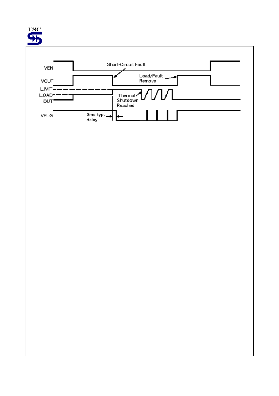
Thermal Shutdown
Thermal shutdown is employed to protect the device from damage should the die temperature exceed safe margins due
mainly to short circuit faults. Each channel employs its own thermal sensor. Thermal shutdown shuts off the output
MOSFET and asserts the FLG output if the die temperature reaches 140
o
C and the overheated channel is in current
limit. The over channel will be shut off. Upon determining a thermal shutdown condition. The TS2026 will automatically
reset its output when the die temperature cools down to 120
o
C . The TS2026 output and FLG signal will continue to
cycle on and off until the device is disabled or the fault is removed. Figure 1. Depicts typical timing. Depending on PCB
layout, package, ambient temperature, etc., it may take several hundred milliseconds from the incidence of the fault to
the output MOSFET being shut off. This time will be shortest in the case of dead short on the output.
Power Dissipation
The device's junction temperature depends on several factors such as the load, PCB layout, ambient temperature and
package type. Equations that can be used to calculate power dissipation of each channel and junction temperature are
found below.
P
D
= R
DS(ON)
x I
OUT
2
Total power dissipation of the device will be the summation of PD for both channels. To relate this to junction
temperature, the following equation can be used:
T
J
= P
D
x
JA
+ T
A
Where:
T
J
= junction temperature
T
A
= ambient temperature
JA
= is the thermal resistance of the package
Current Sensing and Limiting
The current-limit threshold is preset internally. The preset level prevents damage to the device and external load but still
allows a minimum current of 500mA to be delivered to the load. The current-limit circuit senses a portion of the output
MOSFET switch current. The current-sense resistor shown in the block diagram is virtual and has no voltage drop. The
reaction to an over current condition varies with three scenarios.
Switch Enable into Short-Circuit
If a switch is enabled into a heavy load or short-circuit, the switch immediately enters into a constant-current mode,
reducing the output voltage. The FLG signal is asserted indicating an over current condition.
Switch Enable Applied to Enabled Output
When a heavy load or short-circuit is applied to an enabled switch, a large transient current may flow until the current
limit circuitry responds. Once this occurs the device limits current to less than the short circuit current limit specification.
Current-Limit Response-Ramped Load
The TS2026 current-limit profile exhibits a small fold back effect of about 200mA. Once this current-limit threshold is
exceeded the device switches into a constant current mode. It is important to note that the device will supply current up
to the current-limit threshold
Fault Flag
The FLG signal is an N-channel open-drain MOSFET output. FLG is asserted (active-low) when either an over current
or thermal shutdown condition occurs. In the case of and over current condition, FLG will be asserted only after the flag
response delay time, t
D
, has elapsed. This ensured that FLG is asserted only upon valid over current conditions and that
erroneous error reporting is eliminated. For example, false over current condition can occur during hot plug event when
a highly capacitive load is connected and causes a high transient inrush current that exceeds the current-limit threshold
for up to 1ms. The FLG response delay time t
D
is typically 3ms.
Undervoltage Lockout
Undervolrage lockout (UVLO) prevents the output MOSFET from turning on until VIN exceeds approximately 2.5V.
Undervoltage detection function only when the switch is enabled.