TS2207A/B series
1-6
2003/12 rev. B
TS2207A/B
Li-Ion Battery Protector
Ideal for One-Cell Rechargeable
Li-Ion Battery
General Description
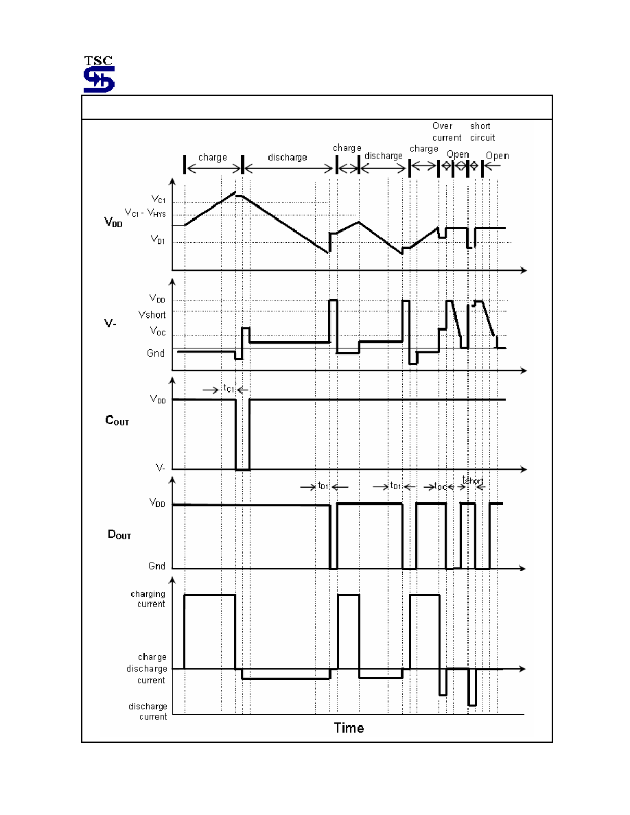
The TS2207A/B series are protection ICs design to safe guard one-cell Lithium-ion battery pack against over
charge/discharge, over current and short circuit. The TS2207A/B series use advanced high voltage CMOS process to
provide high accuracy voltage detection and low current consumption.
The TS2207A/B series incorporate a reference unit and three voltage detectors. During charging process, when the cell
voltage(V
DD
) is charged to a value higher than the over-charge threshold voltage (V
C1
), the over charge detector (COM1)
will switch the output pin (C
OUT
) to a low level within a delay time (t
C1
), and thus turning off the MOSFET connected to the
charging path. The C
OUT
pin may change to high level again when the V
DD
voltage falls below "V
C1
-V
HYS
", or when V
DD
falls below V
C1
while the charger is disconnected from the battery pack.
During the discharging process, when the V
DD
voltage drops to a value lower than the over-discharge threshold voltage
(V
D1
), the over-discharge detector (COM2) will switch D
OUT
to low level within a delay time (t
D1
), and thus turning off the
MOSFET connecting the discharging path. In the mean time, the TS2207A/B series will enter a low current standby
mode. Once into standby mode, the system can only be released from standby mode right after the battery pack is
connected to a charger.
The conditions of over current and short circuit protection are both determined by the voltage at the V- pin. As the voltage
of V- pin reaches a higher value than V
OC
, which indicates an undesirable large current is flowing through the path, D
OUT
will be switched to a low level and the path is cutoff after internally pre-set delay time (t
OC
) elapses. In the case of short
circuit, i.e. V- rises above V
SHORT
, the path will also be cutoff but with almost no delay time. Once the over current or
factors contributing to short circuit is removed, the built-in resistor at the V- pin, typically 100k, will pull V- down to V
SS
and bringing the IC back to normal operation.
Together with the application circuit, the TS2207A/B will function as a consummate protector, which promotes safe usage
and the sustainability of Li-ion battery packs.
Ordering Information
Note: Marking B
XX
,
XX
is wafer and assembly lot code (A~Z & 1~9)
Part No.
Threshold Voltage
Reel
TS2207ACX6
4.30V ~ 4.40V
Black
TS2207BCX6
4.23V ~ 4.33V
White
Features
Low current consumption
Supply current 3uA (typ) and standby current 0.6uA
High withstand voltage up to 22V (VDD ~ V-)
High accuracy voltage detection
Over charge detector: � 50mV
Over discharge detector: � 3.2%
Over current and short circuit protection
Small package of SOT-26
Applications
Over-charge and over-discharge protection for Li-ion
cell pack
High precision protectors for cell-phones and other
gadget using on board Li-ion cell battery
Pin Description
No. Symbol
Description
1
D
OUT
Output of over discharge detection
2
V
-
Pin for charger negative input
3
C
OUT
Output of over charge detection
4
C
EXT
Pin for external capacitor Setting
COM1 delay time
5
V
DD
Power supply
6
V
SS
Ground
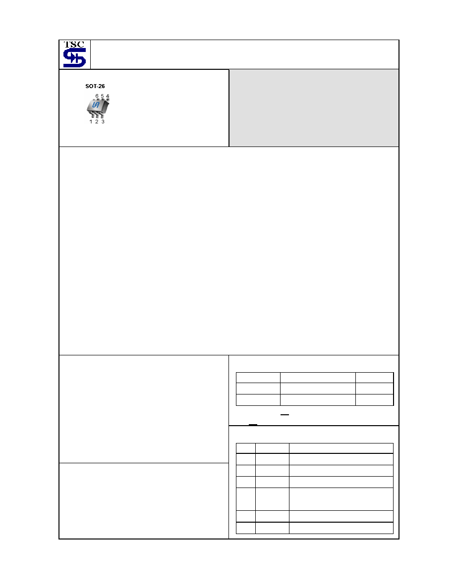
Pin assignment
1. D
OUT
2. V
-
3. C
OUT
4. C
EXT
5. V
DD
6. V
SS
TS2207A/B series
2-6
2003/12 rev. B
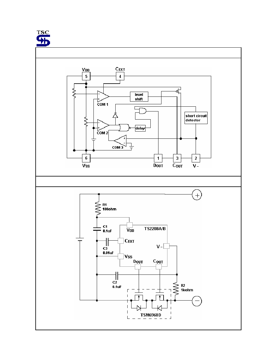
Block Diagram
Typical Application
TS2207A/B series
3-6
2003/12 rev. B
Absolute Maximum Rating
Supply Voltage
V
DD
-0.3 to 12
V
V
-
pin
V-
V
DD
-22 to V
DD
+0.3
V
Input Voltage
V
CT
pin
VCext
V
SS
-0.3 to V
DD
+0.3 V
C
OUT
pin
VC
OUT
V
DD
-22 to V
DD
+0.3 V
Output Voltage
D
OUT
pin
VD
OUT
V
SS
-0.3 to V
DD
+0.3 V
Power Dissipation
P
D
150 mW
Operating Temperature Range
T
OPT
-40 to +85
o
C
Storage Temperature Range
T
STG
-50 to +120
o
C
Note:
Absolute Maximum ratings are threshold limit values that must not be exceeded even for an instant under any
conditions. Operation above these absolute maximum ratings may cause degradation or permanent damage to the
device. These are stress ratings only and do not necessarily functional operation below these limits.
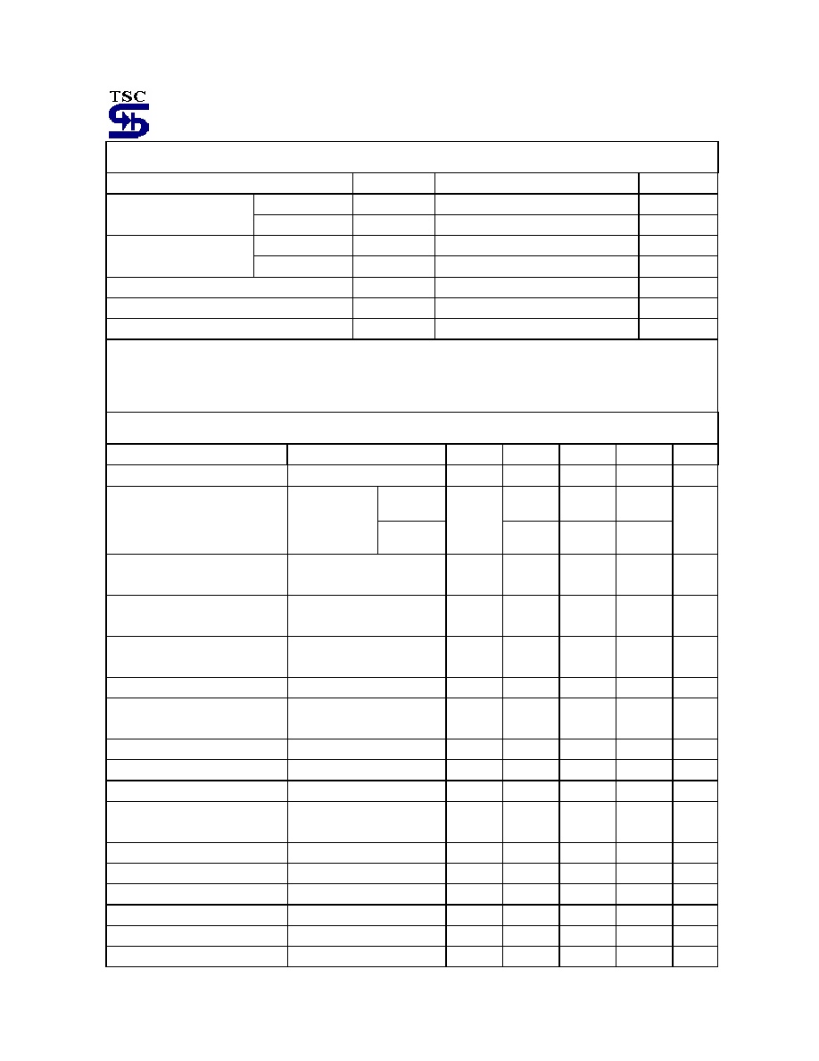
Electrical Characteristics
(Ta = 25
o
C, unless otherwise specified.)
Parameter Conditions
Symbol
Min
Typ
Max
Unit
Operating input voltage
Voltage defined as V
DD
-V
SS
V
DD1
1.5 -- 10 V
TS2207A
4.30 4.35 4.40
Over-charge threshold voltage
Detect rising
edge of supply
voltage
TS2207B
V
C1
4.23 4.28 4.33
V
Over-charge threshold hysteresis
range
V
HYS
0.15 0.20 0.25 V
Over-charge delay time
C
3
= 0.01�F,
V
DD
= 3.6V to 4.4V
t
C1
40 75 145
ms
Over-discharge threshold voltage
Detect falling edge of supply
voltage
V
D1
2.42 2.500 2.58 V
Over-discharge delay time
V
DD
= 3.6V to 2.4V
t
D1
4 10 20
ms
Over current detection voltage
Detect rising edge of "V-" pin
voltage
V
OC
0.17 0.20 0.23 V
Over current detection delay time V
DD
= 3.0V
t
OC
6 13 35
ms
Short circuit detection voltage
V
DD
= 3.0V
Vshort
V
DD
-1.2 V
DD
-0.9 V
DD
-0.6 V
Short circuit detection delay time
V
DD
= 3.0V
tshort
--
5
50
�S
Reset resistance for excess
current protection
V
DD
= 3.6V,V-=1.0V
Rshort
50
100
150
K
Nch ON voltage of C
OUT
I
OL
= 50�A, V
DD
= 4.4V
V
OL1
-- 0.3 0.5 V
Pch ON voltage of C
OUT
I
OH
= -50�A, V
DD
= 3.9V
V
OH1
3.4 3.8 -- V
Nch ON voltage of C
OUT
I
OH
= 50�A, V
DD
= 2.4V
V
OL2
-- 0.2 0.5 V
Pch ON voltage of C
OUT
I
OH
= -50�A, V
DD
= 3.9V
V
OH2
3.4 3.7 -- V
Supply current
V
DD
= 3.9V,V-= 0V
I
DD
-- 3 7 �A
Standby current
V
DD
= 2.0V
I
standby
-- -- 0.6 �A
TS2207A/B series
4-6
2003/12 rev. B
Operation Description
COM1 (Over-Charge Detector)
COM1 is the monitor of the voltage at the V
DD
pin. COM1 senses an over charging condition and if this condition
continues longer than the delay time (t
C1
), When the voltage at V
DD
exceeds the over charge detector threshold V
C1
.
the C
OUT
pin goes to a "L" level thus turns off the external charge control N-ch MOSFET. An internal level shifter is
incorporated in the buffer driver at the C
OUT
pin to drive the "L" level of C
OUT
equal to the V- pin voltage. By the way,
the "H" level of C
OUT
is set equal to V
DD
.
The delay time (t
C1
) of over-charging is decided by the external capacitor C
3
connected between the Vss and Cext pin,
it can be estimated as
t
C1
= [C
3
x (V
DD
-0.7)] / (0.48 x 10
-6
)
. However, if the over-charge condition is not long enough
to cover the time delay window, C
OUT
will not go "L" and the charging process continues.
Required Conditions to Reset COM1 from Over Charging
After the MOSFET, the charge control is turns off, COM1 can be reset under two conditions. As resetting COM1
means C
OUT
returns to "H" again and the charging path is reconnected to restart of charging process. One of the
condition to reset COM1 is when V
DD
falls to lower than "V
C1
- V
HYS
" as a result of battery cell internal discharge.
Disconnecting the battery pack from the charger can also reset COM1 even when V
DD
is still within the hysteresis
window (V
C1
- V
HYS
V
DD
< V
C1
).
After the battery pack is disconnected from the charger, connecting a system load to the battery pack allows current to
flow through the parasitic diode of external charge control MOSFET. This discharging current will bring V
DD
down a
little over some time and once V
DD
drops below V
C1
, C
OUT
will become "H".
COM2 (Over-Discharge Detector)
COM2 monitors the cell voltage at the V
DD
pin. When V
DD
drops below the over-discharge threshold V
D2
during the
discharging process, COM1 senses an over-charging condition and after delay time (t
D1
), the D
OUT
pin goes to a "L"
level and thus turning off the external discharge control N-ch MOSFET. As soon as this happens, the V- pin will be
pulled "H" by an internal PMOS and TS2207A/B series will be enter a standby mode.
Connecting the battery pack to a charger is a necessary condition for TS2207A/B series to recover from standby
mode. With the charger connected, the charge current can flow through the parasitic diode of the external discharge
control N-ch MOSFET while V
DD
is still lower than the over-discharge threshold. Once V
DD
is charged up to a value
higher than V
D1
, the D
OUT
pin goes "H". This leads to the "ON" state of both the charge and discharge control
MOSFETs, and the charge process proceeds on as long as the charger is connected. Connecting a charger to the
battery pack when V
DD
voltage is already higher then V
D1
will make D
OUT
instantaneously "H".
COM3 (Over Current Detector, Short Circuit Protector)
The over current detector and short circuit protector can work when both the charge and discharge control N-ch
MOSFETs are "ON".
Under normal operation, the V- pin voltage will be either slightly higher or lower than Vss (dependent on the
impedance of the two MOSFETs). However, when the V- pin voltage rises to a value between the short protection
voltage Vshort and over current threshold V
OC
, the TS2207A/B series detect an excess current condition. As a result,
the external discharge control N-ch MOSFET goes "OFF" with the D
OUT
pin being at "L". An output delay time for the
over current detection is internally fixed. A quick recovery of V- from a value between Vshort and V
OC
to the normal
value within the delay time keeps the discharge control FET staying at the "ON" state.
Short circuit may as well be explained as a "serious" over current condition. When the V- pin voltage rises to a value
not only higher than V
OC
but also higher than Vshort, the short circuit protector will shut the discharge MOSFET down
immediately to protect battery pack from being damaged or exploding.
The V- pin has a built-in pull down resistor. Thus once the cause of over current or short circuit is removed, the V- pin
will be pulled down to the ground level through the internal resistor. Therefore, with V- lower than the over current and
short circuit protection threshold, D
OUT
will be turned back on and the TS2207A/B series can continue normal charge
or discharge operation.
When over current or short circuit occurs, the TS2207A/B series will not enter a standby mode.
TS2207A/B series
5-6
2003/12 rev. B
Timing Diagram
TS2207A/B series
6-6
2003/12 rev. B
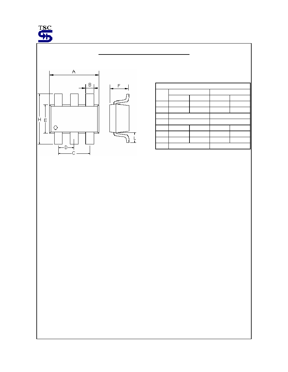
SOT-26 Mechanical Drawing
SOT-26 DIMENSION
MILLIMETERS INCHES
DIM
MIN MAX MIN MAX
A 2.70 3.00 0.106 0.118
B 0.25 0.50 0.010 0.020
C 1.90(typ)
0.075(typ)
D 0.95(typ)
0.037(typ)
E 1.50 1.70 0.059 0.067
F 1.05 1.35 0.041 0.053
H 2.60 3.00 0.102 0.118
L 0.60(typ)
0.024(typ)