TS2411
1-6
2004/09 rev. B
TS2411
Tong Ringer
Operating Voltage 13 to 36V
Ringing Start Voltage 36V (max.)
General Description
The TS2411 is a bipolar integrated circuit designed for telephone bell replacement.
Features
Designed for Telephone Bell Replacement
Low Current Drain
Adjustable 2-frequency Tone
Adjustable Warbling Rate
Extension Tone Ringer Modules
Alarms or Other Alerting Devices
Adjustable for Reduced Supply Initiation Current.
Built-in hysteresis prevents false triggering and rotary
dial `Chirps'
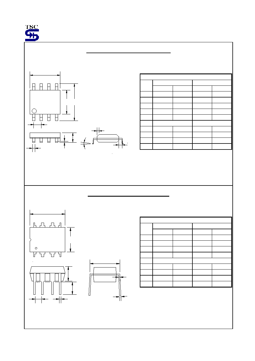
Ordering Information
Part No.
Operating Temp.
Package
TS2411CD
DIP-8
TS2411CS
-20 ~ +70
o
C
SOP-8
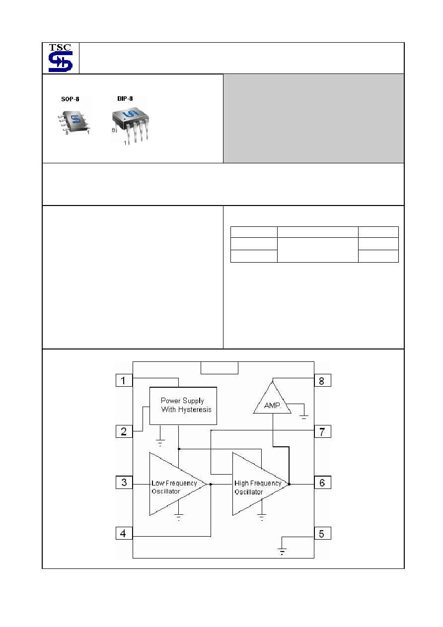
Block Diagram
Pin assignment:
1. Vcc 5. Gnd
2. Rsl 6. Hfo
3. Lfi 7. Hfi
4. Lfo 8. Out
TS2411
2-6
2004/09 rev. B
Absolute Maximum Rating
Description Symbol
Value
Unit
DC Supply Voltage (Referenced to GND)
VCC
+ 36
V
Power Dissipation in Still Air Plastic DIP
PD
400
mW
Switch Collector Voltage
Tstg
-65 to +150
o
C
Note:
* Maximum Ratings are those values beyond which damage to the device may occur.
Functional operation should be restricted to the Recommended Operating Conditions.
Recommended Operating Conditions
Description Symbol
Min
Max
Unit
Operating Voltage
Vopr
13 36 V
Operating Temperature
T
A
-45 +65
o
C
Note:
This device contains protection circuitry circuitry to guard against damage due to high static voltages or electric
fidlds. However, precautions must be taken to avoid applications of any voltage higher than maximum rated voltages to
this high-impedance circuit. For proper operation, V
IN
and V
OUT
should be constrained to the range
GND(V
IN
or V
OUT)
Vcc.
Unused inputs must always be tied to an appropriate logic voltage level (e.g.,either GND or Vcc). Unused outputs must
be left open.
Electrical Characteristics
(Voltages Referenced to GND,T
A
=-20 to +70
o
C)
Parameter
Symbol
Test Conditions
Min
Typ
Max
Unit
Initiation Supply Voltage (1)
V
SI
See Figure 2
16.8
--
21.2
V
Initiation Supply Current (1)
I
SI
See Figure 2
1.4
--
4.2
mA
Sustaining Voltage (1)
V
SUS
See Figure 2
9.5
--
12.2
V
Sustaining Current
I
SUS
See Figure 2
0.7 -- 2.5 mA
High-Level Output Voltage
V
OH
Vcc=21V,I
OH
=-15mA,
Pin6=6V, Pin7=GND
16.7 -- 21.0 V
Low-Level Output Voltage
V
OL
Vcc=21V,I
OL
=15mA,
Pin6= GND, Pin7=6V
-- -- 1.8 V
Pin3 =6V, Pin4 =GND, Vcc=21V
--
--
1.0
A
Maximun Input Leakage Current
I
IN
Pin7 =6V, Pin6 =GND, Vcc=21V
--
--
1.0
A
High Frequency 1
F
H1
R
3
=191K,C
3
=6800pF
461 -- 563 H
Z
High Frequency 2
F
H2
R
3
=191K,C
3
=6800pF
576 -- 704 H
Z
Low Frequency
F
L
R
2
=165K,C
2
=0.47uF
9.0
--
11.0
H
Z
Ringing Start Voltage (4)
Vtr
See Figure 1
--
--
36
V
Notes
: 1. Initiation supply voltage (V
SI
) is the supply voltage required to start the tone ringer oscillating.
2. Sustaining voltage (V
SUS
) is the supply voltage required to maintain oscillation.
3. Ringing start voltage is the value of AC supply voltage required to start the tone ringer ringing in FIG.3
4. This product is not designed for protection against radioactive rays.
5. All data and specifications are subject to change without notice.
TS2411
3-6
2004/09 rev. B
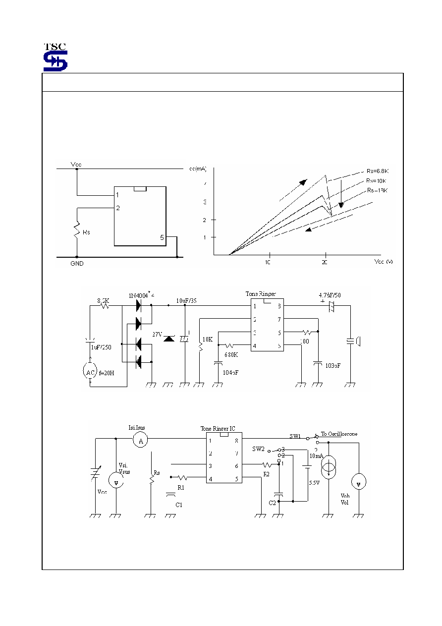
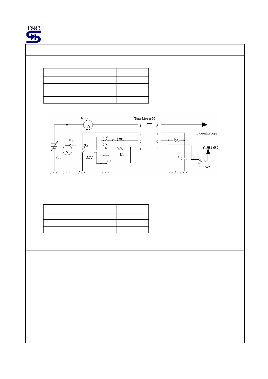
Application Circuit
.
HOW TO USE THE RSL PIN
In the IC, the supply initiation current (lsi) can be changed using the RSL Pin. As show is the diagram, the RSL (Pin 2)
is grounded through resistor Rs. By changing the Rs value, supply initiation current can be changed.
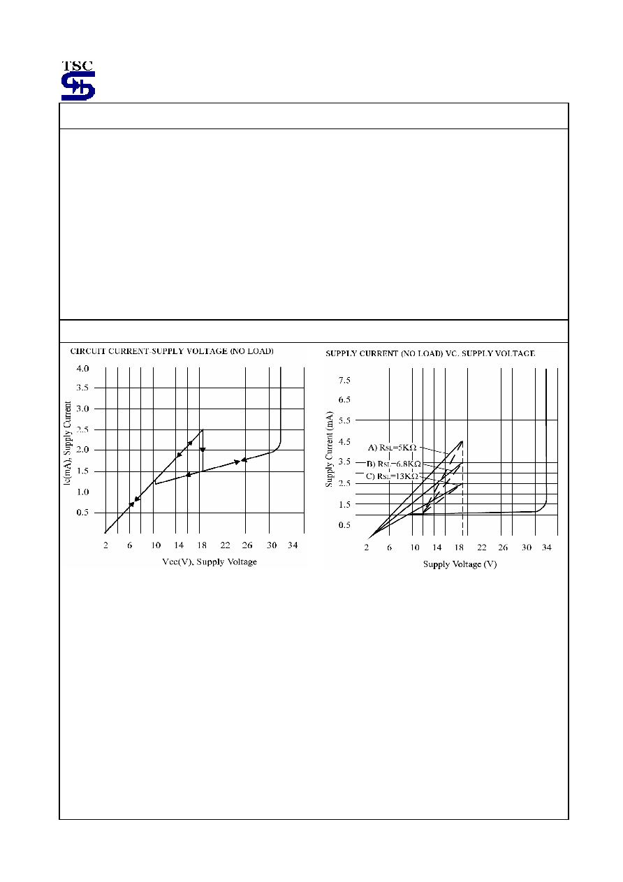
Supply voltage (Vcc) vs. supply current (lcc) characteristics resulting from changes in the value of Rs are shown in the
following diagram.
Figure 1. Ringing Start Voltage Test Circuit
Figure 2. Test Circuit (1)
TS2411
4-6
2004/09 rev. B
Application Circuit
SWITCH POSITION IS THE FOLLOWING TABLE: :
PARAMETER SW1 SW2
Vsi , Isi
1
1
Vsus , Isus
1
1
Voh
2
2
Vol 2
3
Figure 3. Test Circuit (2)
SWITCH POSITION IS THE FOLLOWING TABLE :
PARAMETER SW1 SW2
FL 1
1
fH1 3
2
fH2 2
2
Application Note
The application circuit illustrates the use of the TS2411 devices in typical telephone or extension tone ringer
application.
The AC ringer signal voltage appears across the TIP and RING inputs of the circuit and is attenuated by capacitorC1
and resistor R1.
C1 also provides isolation from DC voltages (48V) on the exchange line.
After full wave rectification by the bridge diode, the waveform is filtered by capacitor C4 to provide a DC supply
for the tone ringer chip. As this voltage exceeds the initiation voltage (VSI), oscillation starts.
With the components shown, the ouptut frequency chops between 512(fh1) and 640Hz(fh2) at a 10Hz(fL) rate.
The loudspeaker load is coupled through a 1300W to 8W transformer.
The output coupling capacitor C5 is required with transformer coupled loads.
When driving a piezo-ceramic transducer type load, the coupling C5 and transformer (1300W:8W) are not required.
However, a current limiting resistor is required.
The low frequency oscillator oscillates at a rate (fL) controlled by an external resistor (R2) and capacitor (C2).
The frequency can be determined using the relation fL=1/1.289R2*C2. The high frequency oscillates at a fH1, fH2
controlled by an external resistor (R3) and capacitor (C3). The frequency can be determined using the relation
H1=1/1.504R3*C3, fH2=1/1.203R3*C3.
R1 = 165 K (+/-) 1%
R2 = 191 K (+/-) 1%
C1 = 0.47
�F (+/-) 5%
C2 = 0.0068
�F (+/-) 5%
R1 = 165 K (+/-) 1%
R2 = 191 K (+/-) 1%
C1 = 0.47
�F (+/-) 5%
C2 = 0.0068
�F (+/-) 5%
TS2411
5-6
2004/09 rev. B
Application Note
Pin 2 allows connection of an external resistor RSL, which is used to program the solpe of the supply current vs
supply voltage characteristics (see Fig2), and hence the supply current up to the initiation voltage ( VSI ). This
initiation voltage remains constant independent of RSL.
The supply current drawn prior to triggering varies inversely with RSL, decreasing for increasing value of
resistance. Thus, increasing the value of RSL will decrease the amount of AC ringing current required to trigger the
device. As such, longer sucribser loops are possible since less voltage is dropped per unit length of loop wire due to
the lower current level. RSL can also be used to compensated for smaller AC couplin capacitors (C5 on Fig 3)
(higher impedance) to the line which can be used to alter the ringer equivalence number of a tone ringer circuit.
The graph in Fig2 illustrates the variation of supply current with supply voltage. Three curves are drawn to show
the variation of initiation current with RSL. Curve B( RSL=6.8KW) shows the I-V characteristic for the TS2411 tone
ringer.
Curve A is a plot with RSL<6.8KW and shows an increase in the current drawn up to the initiation voltage VSI. The
I-V characteristic after initiation remains unchanged. Curve C illustrates the effect of increasing RSL above 6.8KW
initiation current decreases but again current after triggering is unchanged.
Characteristics Curve
Figure 4.
Figure 5.