 | –≠–ª–µ–∫—Ç—Ä–æ–Ω–Ω—ã–π –∫–æ–º–ø–æ–Ω–µ–Ω—Ç: TS2576 | –°–∫–∞—á–∞—Ç—å:  PDF PDF  ZIP ZIP |
TS2576 1-7
2003/12
rev.
A
TS2576
3A Step Down Switching Voltage Regulator
Pin assignment:
1. Input
2. Output
3. Ground
4. Feedback
5. Enable
52KHz Oscillating Frequency
Output Current up to 3A
Enable Input Control
General Description
The TS2576 Series are step-down switching regulators with all required active functions. It is capable of driving 3A load
with excellent line and load regulations. These devices are available in fixed output voltages of 3.3V, 5V, and an
adjustable output version.
The TS2576 series offers a high-efficiency replacement for popular three-terminal linear regulators. Also it requires a
minimum number of external components. It substantially not only reduces the area of board size but also the size of heat
sink, and in some cases no heat sink is required. The ±4% tolerance on output voltage within specified input voltages and
output load conditions is guaranteed. Also, the oscillator frequency accuracy is within ±10%. External shutdown is
included. Featuring 70µA (typical) standby current. The output switch includes cycle-by-cycle current limiting, as well as
thermal shutdown for full protection under fault conditions.
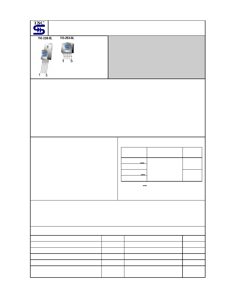
This series are offered in 5-pin TO-263, TO-220 package.
Features
Guaranteed 3A output current
3.3V, 5V, and adjustable versions
Wide input voltage range, up to 40V
Internal oscillator of 52KHz fixed frequency
Wide adjust version output voltage range, from 1.23V
to 37V ±4% max. at over line and load conditions.
Low standby current, typ. 70µA, at shutdown mode
Requires only 4 external components
Thermal shutdown and current limit protection
P+ product enhancement tested
Ordering Information
Note: Where
xx
denotes voltage option, available are
12V, 5V and 3.3V. Leave blank for adjustable
version. Contact factory for additional voltage
options.
Part No.
Operating Temp.
(Ambient)
Package
TS2576CZ5-
xx
TS2576CZ5
TO-220-5L
TS2576CM5-
xx
TS2576CM5
-20 ~ +85
o
C
TO-263-5L
Applications
LCD
Monitors
ADD-ON Cards Switching Regulators
High Efficiency Step-Down Regulators
Efficient Pre-regulator for Linear Regulators
Positive to Negative converter (Buck-Boost)
Absolute Maximum Rating
Input Voltage
Vin
+45
V
ENABLE Pin Input Voltage
Vin (operate)
-0.3V V Vin
V
Power Dissipation
P
D
Internal
Limited W
Operating Junction Temperature Range
T
J
-0 ~ +150
o
C
Storage Temperature Range
T
STG
-65 ~ +150
o
C
Lead Soldering Temperature (260
o
C)
TO-220-5L / TO-263-5L Package
5
S
TS2576 2-7
2003/12
rev.
A
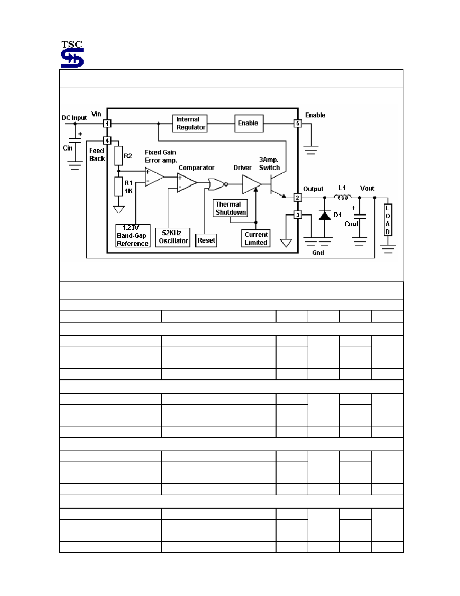
Block Diagram
Electrical Characteristics
Vin = 12V, I
L
= 500mA, Ta = 25
o
C unless otherwise specified.
Parameter Conditions
Min
Typ
Max
Unit
TS2576-3.3V
Output Voltage (Note 1)
Vin=12V, I
L
=0.5A (Figure 1)
0.98|Vo|
1.02|Vo|
Output Voltage (Note 1)
0.5A
I
L
3A, 6V Vin 40V
(Figure 1)
0.96|Vo|
3.3
1.04|Vo|
V
Efficiency
Vin=12V, I
L
=3A --
75
--
%
TS2576-5V
Output Voltage (Note 1)
Vin=12V, I
L
=0.5A(Figure 1)
0.98|Vo|
1.02|Vo|
Output Voltage (Note 1)
0.5A
I
L
3A, 8V Vin 40V
(Figure 1)
0.96|Vo|
5.0
1.04|Vo|
V
Efficiency
Vin=12V, I
L
=3A --
77
--
%
TS2576-12V
Output Voltage (Note 1)
Vin=25V, I
L
=0.5A (Figure 1)
0.98|Vo|
1.02|Vo|
Output Voltage(Note 1)
0.5A
I
L
3A, 15V Vin 40V
(Figure 1)
0.96|Vo|
12
1.04|Vo|
V
Efficiency
Vin=15V, I
L
=3A --
88
--
%
TS2576
Feedback Voltage (Note 1)
Vin=12V, Vout=5V,I
L
=0.5A (Figure 2)
0.98|Vo|
1.02|Vo|
Feedback Voltage (Note 1)
0.5A
I
L
3A, 8V Vin 40V,
Vout=5V (Figure 2)
0.96|Vo|
1.23
1.04|Vo|
V
Efficiency
Vin=12V, Vout=5V, I
L
=3A --
77
--
%
TS2576 3-7
2003/12
rev.
A
All Output Voltage Version
(Vin=12V for 5V, 3.3V and Adjustable version, Vin=25V for 12V version, I
L
= 500mA)
Oscillator Frequency (Note 2)
47
52
58
kHz
Quiescent Current (Note 3)
--
5
10
mA
Standby Current
ENABLE =5V
--
70
200
uA
Saturation Voltage (Note 4)
I
LOAD
=3A --
1.4
1.8
V
Feedback Bias Current
V
OUT
=5V (Adj. Version only)
--
50
100
nA
Duty Cycle (Note 5)
Operating (ON)
93
98
--
%
Current Limit (Note 2)(Note 4)
4.2
7.0
8.8
A
V
OUT
=0V --
0.3
2
Output Leakage Current (Note 3)
V
OUT
=-1V --
7.5
30
mA
V
IH
(V
OUT
=0V) 2.2
1.4
--
ENABLE Threshold Voltage
V
IL
(V
OUT
=Normal Output Voltage)
--
1.2
1.0
V
I
IH
(ENABLE =5V)
--
12
30
ENABLE Input Current
I
IH
(ENABLE =0V)
--
0
10
uA
Note 1: External components such as the catch diode, inductor, input and output capacitors can affect switching regulator
system performance. Refer to Application information for details.
Note 2: The oscillator frequency reduces to approximately 11KHz in the event of fault conditions, such as output short or
overload. And the regulated output voltage will drop approximately 40% from the nominal output voltage. This
self-protection feature lowers the average power dissipation by lowering the minimum duty cycle from 5% down to
approximately 2%.
Note 3: For these parameters, FB is removed from V
OUT
and connected to +12V to force the output transistor OFF.
Note 4: V
OUT
pin sourcing current. No diode, inductor or capacitor connected to V
OUT.
Note 5: FB is removed from V
OUT
and connected to 0V.
TS2576 4-7
2003/12
rev.
A
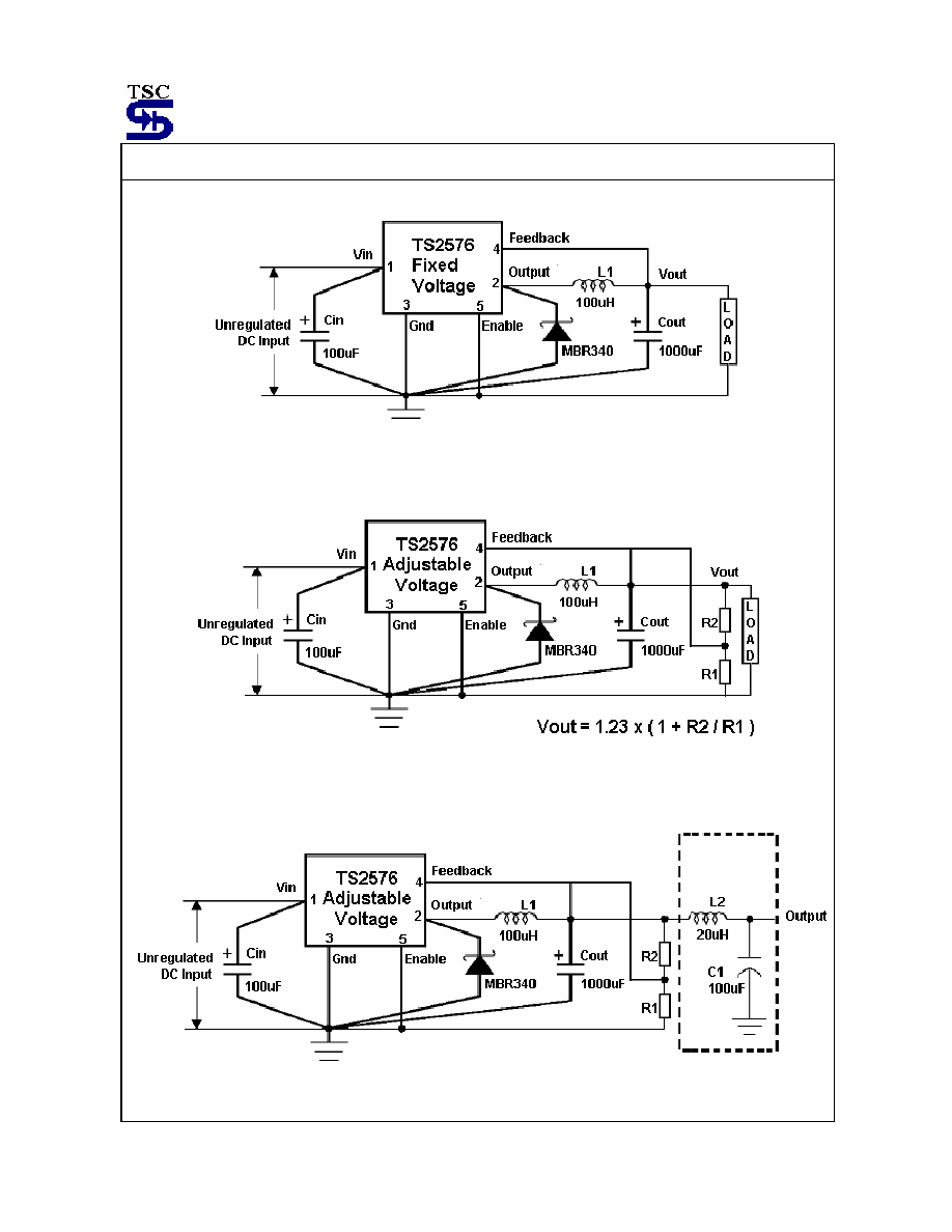
Typical Application Circuit
Figure 1 Fixed Voltage Version
Figure 2: Adjustable Voltage Version
Figure 3: LC filter for Low Output Ripple
TS2576 5-7
2003/12
rev.
A
Application Information
It is required that VIN must be bypassed with at least a
100µF electrolytic capacitor for stability. Also, it is
strongly recommended the capacitor's leads must be
dept short, and located near the regulator as possible.
For low operating temperature range, for example, below
-25
o
C, the input capacitor value may need to be larger.
This is due to the reason that the capacitance value of
electrolytic capacitors decreases and the ESR increases
with lower temperatures and ago. Paralleling a ceramic
or solid tantalum capacitor will increase the regulator
stability at cold temperatures.
Output Capacitor
An output capacitor is also required to filter the output
voltage and is needed for loop stability. The capacitor
should be located near the TS2576 using short PC
board traces. Low ESR types capacitors are
recommended for low output ripple voltage and good
stability. Generally, low value or low voltage (less than
12V) electrolytic capacitors usually have higher ESR
numbers, For example, the lower capacitor values
(220µF - 1000µF) will yield typically 50mV to 150mV of
output ripple voltage, while larger-value capacitors will
reduce the ripple to approximately 20mV to 50mV.
The amount of output ripple voltage is primarily a
function of the ESR (Equivalent Series Resistance) of
the output capacitor and the amplitude of the inductor
ripple current ( I
IND
)
Output Ripple Voltage = ( I
IND
) x (ESR of C
OUT
)
Some capacitors called "high-frequency",
"low-inductance", or "low-ESR" are recommended to use
to further reduce the output ripple voltage to 10mV or
20mV. However, very low ESR capacitors, such as
tantalum capacitors, should be carefully evaluated.
Catch Diode
This diode is required to return path for the inductor
current when the switch is off. It should be located close
to the TS2576 using short leads and short printed circuit
traces as possible.
To satisfy the need to fast switching speed and low
forward voltage drop, Schottky diodes are widely used to
provide the best efficiency, especially in low output
voltage switching regulators (less than 5V). Beside,
Fast-Recovery, high-efficiency, or ultra fast recovery
diodes are also suitable. But some types with an abrupt
turn-off characteristic may cause instability and EMI
problems. A fast recovery diode with soft recovery
characteristics is better choice.
Inductor Selection
The TS2576 can be used for either continuous or
discontinuous modes of operation. Each mode has
distinctively different operating characteristics, which can
affect the regulator performance and requirements.
With relatively heavy load currents, the circuit operates
in the continuous mode (inductor current always flowing).
But under light
Load conditions, the circuit will be force to the
discontinuous mode (inductor current falls to zero for a
period of time). For light loads (less than approximately
300mA) it may be desirable to operate the regulator in
the discontinuous mode, primarily because of the lower
inductor values required for the discontinuous mode.
Indictors are available in different styles such as pot
core, toroid, E-frame, bobbin core, et., as well as
different core materials such as ferrites and powdered
iron. The least expensive, the bobbin core type, consists
of wire wrapped on a ferrite rod core. This type of
construction makes for an inexpensive inductor, but
since the magnetic flux is not completely contained
within the core, it generates more electromagnetic
interference (EMI). This EMI can cause problems in
sensitive circuits, or can give incorrect scope readings
because of induced voltage in the scope probe. An
inductor should not be operated beyond its maximum
rated current because it may saturate. When an inductor
begins to saturate, the inductance decreases rapidly and
the inductor begins to look mainly resistive (the DC
resistance of the winding). This will cause the switch
current to rise very rapidly. Different inductor types have
different saturation characteristics, and this should be
well considered when selecting as inductor.
Feedback Connection
For fixed output voltage version, the FB (feedback) pin
must be connected to V
OUT
. For the adjustable version, it
is important to place the output voltage ratio resistors
near TS2576 as possible in order to minimize the noise
introduction.
Enable Input
It is required that the ENABLE must not be left open. For
normal operation, connect this pin to a "LOW" voltage
(typically, below 1.6V). On the other hand, for standby
mode, connect this pin with a "HIGH" voltage. This pin
can be safely pulled up to +
VIN
without a resistor in series
with it.