TS2596
1-6
2003/12 rev. D
TS2596
Preliminary
3A Step Down Switching Voltage Regulator
Pin assignment:
1. Input
2. Output
3. Ground
4. Feedback
5. Enable
150KHz Oscillating Frequency
Output Current up to 3A
Enable Input Control
General Description
The TS2596 Series are step-down switching regulators with all required active functions. It is capable of driving 3A load
with excellent line and load regulations. These devices are available in fixed output voltages of 3.3V, 5V, and an
adjustable output version.
The TS2596 series operates at a switching frequency of 150kHz thus allowing smaller sized filter components than what
would be needed with lower frequency switching regulators. It substantially not only reduces the area of board size but
also the size of heat sink, and in some cases no heat sink is required. The ±4% tolerance on output voltage within
specified input voltages and output load conditions is guaranteed. Also, the oscillator frequency accuracy is within ±10%.
External shutdown is included. Featuring 70µA (typical) standby current. The output switch includes cycle-by-cycle current
limiting, as well as thermal shutdown for full protection under fault conditions.
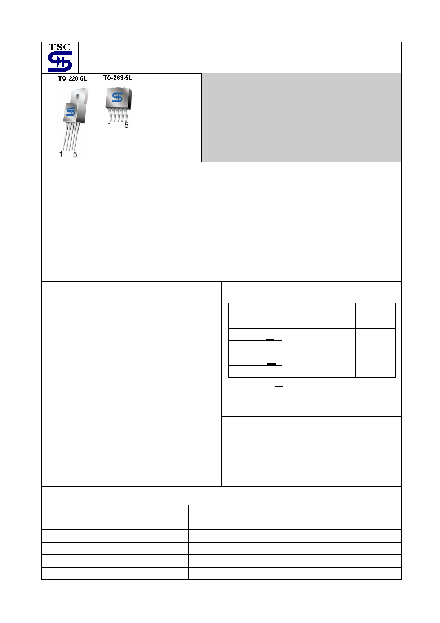
This series are offered in 5-pin TO-263, TO-220 package.
Ordering Information
Note: Where
xx
denotes voltage option, available are
5V and 3.3V. Leave blank for adjustable
version. Contact factory for additional voltage
options.
Part No.
Operating Temp.
(Ambient)
Package
TS2596CZ5
xx
TS2596CZ5
TO-220-5L
TS2596CM5
xx
TS2596CM5
-20 ~ +85
o
C
TO-263-5L
Features
Guaranteed 3A output current
3.3V, 5V, and adjustable versions
Wide input voltage range, up to 40V
Internal oscillator of 150KHz fixed frequency
Wide adjust version output voltage range, from 1.23V
to 25V ±4% max. at over line and load conditions.
Low standby current, typ. 70µA, at shutdown mode
Requires only 4 external components
Thermal shutdown and current limit protection
P+ product enhancement tested
Applications
LCD
Monitors
ADD-ON Cards Switching Regulators
High Efficiency Step-Down Regulators
Efficient Pre-regulator for Linear Regulator
Absolute Maximum Rating
Input Voltage
Vin
+40
V
ENABLE Pin Input Voltage
Vin (operate)
-0.3V V Vin
V
Power Dissipation
P
D
Internal
Limited W
Operating Junction Temperature Range
T
J
-40 ~ +125
o
C
Storage Temperature Range
T
STG
-65 ~ +150
o
C
Lead Soldering Temperature (260
o
C)
5
S
TS2596
2-6
2003/12 rev. D
Thermal Performance
Condition Symbol
Limits Unit
Thermal Resistance Junction to Ambient
ja 30
Thermal Resistance Junction to Case
jc 3
o
C/W
Recommended Operating Conditions (
Ta = 25
o
C)
Condition Symbol
Limits Unit
Input Voltage
Vin
4.5 ~ 28
V
ENABLE Pin Input Voltage
Vin (operate)
0 ~ +20
V
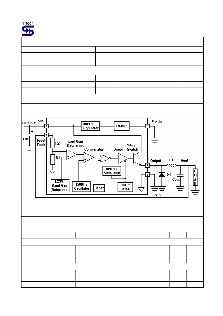
Block Diagram
Electrical Characteristics
Vin = 12V, I
L
= 500mA, Ta = 25
o
C unless otherwise specified.
Parameter Conditions
Min
Typ
Max
Unit
TS2596-3.3V
Output Voltage (Note 1)
0.2A
I
L
3A, 5.07V Vin 40V
(Figure 1)
0.96|Vo|
3.3 1.04|Vo|
V
Efficiency
Vin=12V, I
L
=3A
-- 75 -- %
TS2596-5V
Output Voltage (Note 1)
0.2A
I
L
3A, 8V Vin 40V
(Figure 1)
0.96|Vo|
5.0 1.04|Vo|
V
Efficiency
Vin=12V, I
L
=3A
-- 80 -- %
TS2596
3-6
2003/12 rev. D
Electrical Characteristics
(Continued)
Vin = 12V, I
L
= 500mA, Ta = 25
o
C unless otherwise specified.
TS2596 Adjustable
Feedback Voltage (Note 1)
0.2A
I
L
3A, 8V Vin 40V,
Vout=5V (Figure 2)
0.96|Vo|
1.23 1.04|Vo| V
Efficiency
Vin=12V, Vout=5V, I
L
=3A --
75
--
%
All Output Voltage Version
(Vin= 12V, I
L
= 500mA)
Oscillator Frequency (Note 2)
127
150
173
kHz
Quiescent Current (Note 3)
--
5
10
mA
Standby Current
ENABLE =5V
--
70
200
uA
Saturation Voltage (Note 4)
I
LOAD
=3A --
1.2
1.5
V
Feedback Bias Current
V
OUT
=5V (Adj. Version only)
--
50
100
nA
Duty Cycle (Note 5)
Operating (ON)
93
98
--
%
Current Limit (Note 2)(Note 4)
--
4.5
--
A
V
OUT
=0V --
0.3
2
Output Leakage Current (Note 3)
V
OUT
=-1V --
7.5
30
mA
V
IH
(V
OUT
=0V) 2.0
--
--
ENABLE Threshold Voltage
V
IL
(V
OUT
=Normal Output Voltage)
--
--
0.6
V
I
IH
(ENABLE =5V)
--
12
30
ENABLE Input Current
I
IH
(ENABLE =0V)
--
0
10
uA
Note 1: External components such as the catch diode, inductor, input and output capacitors can affect switching regulator
system performance. Refer to Application information for details.
Note 2: The oscillator frequency reduces when the second stage current limit is activated. The amount of reduction is
determined by the severity of current over load.
Note 3: For these parameters, FB is removed from V
OUT
and connected to +12V to force the output transistor OFF.
Note 4: V
OUT
pin sourcing current. No diode, inductor or capacitor connected to V
OUT.
Note 5: FB is removed from V
OUT
and connected to 0V.
TS2596
4-6
2003/12 rev. D
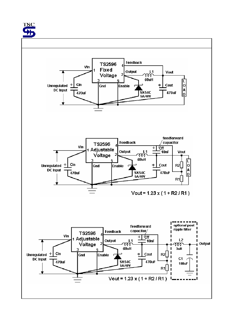
Typical Application Circuit
Figure 1 Fixed Voltage Version
Figure 2: Adjustable Voltage Version
Figure 3: LC filter for Low Output Ripple
TS2596
5-6
2003/12 rev. D
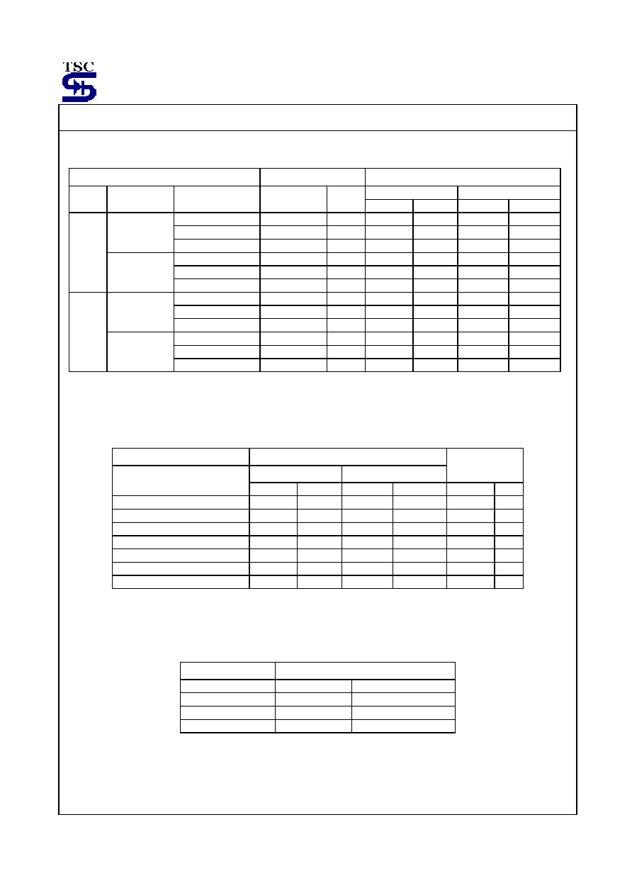
Application Data
Quick Design Component Selection Table for Fixed Output
Input / Output Condition
Inductor
Output Capacitor
Nichicon PL series Sprague 595D series
Output
(V)
Load current
(A)
Max. Input voltage
(V)
Inductance
(uH)
Current
(A)
uF V uF V
8 22
3.5
560
25
330
10
15 33
3.5
330
35
330
10
3
25 47
3.5
270
35
330
10
9 22
3.1
470
25
330
10
15 68
3.1
180
35
270
10
5
2
25 68
3.1
180
35
270
10
5 22
3.5
470
25
390
6.3
12 22
3.5
560
35
390
6.3
3
25 33
3.5
680
35
390
6.3
6 22
3.1
470
25
390
6.3
12 33
3.1
330
35
390
6.3
3.3
2
25 47
3.1
330
35
330
10
Quick Design Component Selection Table for Adjustable Output
Input / Output Condition
Output Capacitor
Nichicon PL series
Sprague 595D series
Feedforword
Capacitor
Output (V)
uF V uF V Value
Unit
2 820
35
330
10
33
nF
4 470
35
330
10
10
nF
6 470
25
330
10
3.3
nF
9 330
25
330
10
1.5
nF
12 330
25
270
10
1
nF
15 220
35
270
10
680
pF
24 150
35
390
6.3
560
pF
Schottky Diode Selection Table
(Taiwan Semiconductor Part Number)
Reverse Voltage
Forward Rectified Current
(4~6A)
(V)
Surface Mount
Through Hole
20 -- SR502
30 SK53C SR503
40 SK54C SR504