TS2902
1-6
2005/04 rev. B
TS2902
Preliminary
Quad Operating Amplifier
Supply Voltage Range 3 V to 26V
Quad Channel Amplifier
General Description
The TS2902 contains four independent high gain operational amplifiers with internal frequency compensation. The
four op-amps use a split power supply. The device has low power supply current drain, regardless or the power
supply voltage. The low power drain also makes the TS2902 a good choice for battery operation.
When your project calls for a traditional op-amp function, now you can streamline your design with a simple single
power supply. Use ordinary +5V common to practically any digital system or personal computer application, without
requiring an extra 15V power supply just to have the interface electronics you need.
The TS2902 is a versatile, rugged workhorse with a thousand-and-one uses, from amplifying signals from a variety of
transducers to dc gain blocks, or any op-amp function. The attached pages offer some recipes that will have your
project cooking in no time.
The TS2902 is offered in 14 pin SOP-14 and DIP-14 package.
Features
Single supply operation: 3V to 32V
Low input bias currents
Internally
compensated
Common mode range extends to negative supply
Single and split supply operation
Ordering Information
Part No.
Operating Temp.
Package
TS2902CD14 DIP-14
TS2902CS14
-40 ~ +85
o
C
SOP-14
Block Diagram
Absolute Maximum Rating
Supply
Voltage
Vcc 26 V
Differential Input Voltage (note 1)
V
IDR
26 V
Input Common Mode Voltage Range (note 2)
Input Forward Current (note 3)
V
ICR
Iif
-0.3 to 26
50
V
mA
Output Short Circuit Duration
Isc
Continuous
mA
Operating Junction Temperature Range
T
J
0 ~ +125
o
C
Storage Temperature Range
T
STG
-65 ~ +150
o
C
NOTE :
1. Split Power Supplies.
2. For supply. Voltages less than 26V for the TS2902 the absolute maximum input voltage is equal to the supply voltage.
3. This input current will only exist when the voltage is negative at any of the input leads. Normal output states will
reestablish when the input voltage returns to a voltage greater than -0.3V.
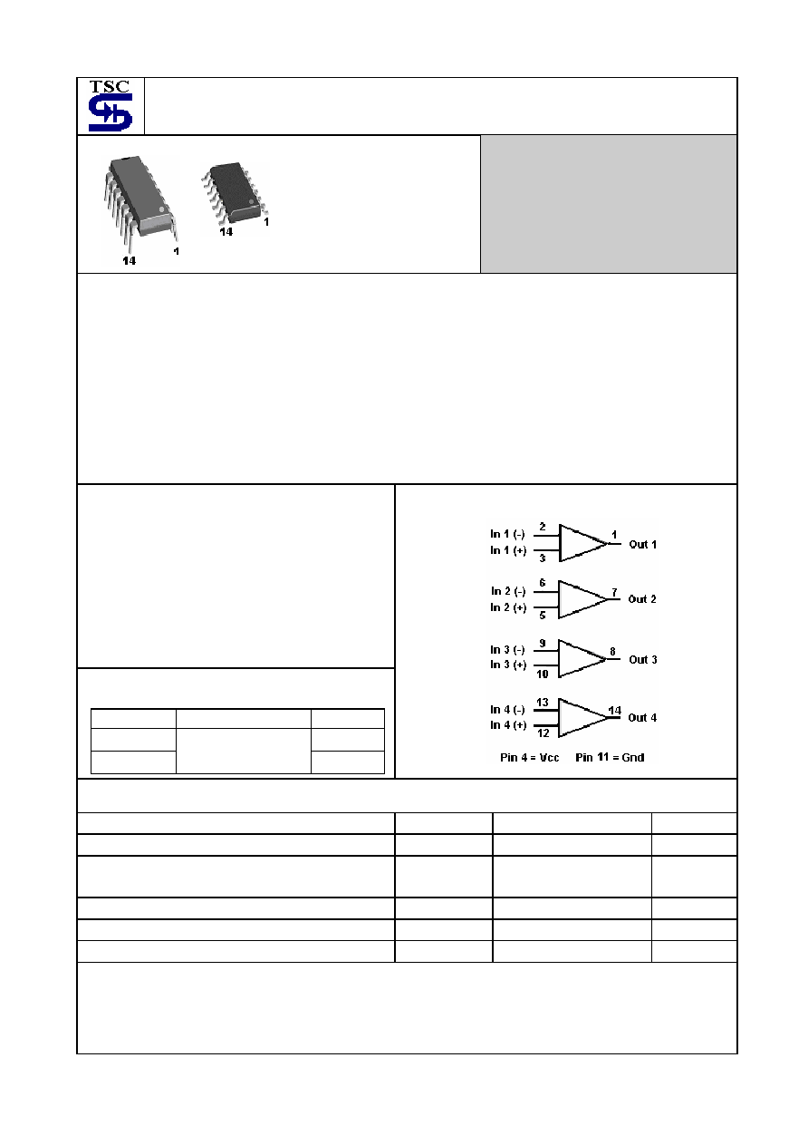
Pin assignment:
1. Output A 14. Output D
2. Input A (-) 13. Input D (-)
3. Input A(+) 12. Input D (+)
4. Vcc
11. Gnd
5. Input B (+) 10. Input C (+)
6. Input B (-)
9. Input C (-)
7. Output B
8. Output C
SOP-14
DIP-14
TS2902
2-6
2005/04 rev. B
Electrical Characteristics
(V
CC
= 5V, Ta=25
o
C; unless otherwise specified.)
Characteristics Symbol
Min
Typ
Max
Unit
Input Offset Voltage
V
CC
= 5.0V to 26V, V
IC
= 0V to Vcc -1.7 V, Vo= 1.4V, R
S
= 0
T
LOW
Ta
T
HIGH
Vio
--
--
2.0
--
7.0
10
mV
Average Temperature Coefficient of Input Offset Voltage
Iio/T -- 7.0 --
uV/
o
C
Input Offset Current
T
LOW
Ta
T
HIGH
Iio
--
--
5.0
--
50
200
nA
Average Temperature Coefficient of input Offset Current
Iio/T
-- 10 --
pA/
o
C
Input Bias Current
T
LOW
Ta
T
HIGH
I
IB
--
90
50
250
500
uA
Input Common-Mode Voltage Range (Note1)
V
CC
= 26 V
V
CC
= 26 V, T
LOW
Ta
T
HIGH
V
ICR
0
0
--
--
24.3
24
V
Differential Input Voltage Range
V
IDR
-- -- V
CC
V
Large Signal Open-Loop Voltage Gain
R
L
= 2.0K, V
CC
=15V, For Large V
O
Swing,
T
LOW
Ta
T
HIGH
A
VOL
--
15
100
--
--
--
V/mV
Channel Separation
1.0 KHz to 20KHz
-- --
-120
--
dB
Common Mode Rejection Ratio
R
S
10 k
CMRR 50 70 -- dB
Power Supply Rejection Ratio
PSRR
50
100
--
dB
Output Voltage -- High Limit
V
CC
= 26 V, R
L
= 2 k
V
CC
= 26 V, R
L
= 10 k
V
OH
22
23
--
24
--
--
V
Output Voltage -- Low Limit
V
CC
= 5.0 V, R
L
= 10 k
V
OL
-- 5.0
100
mV
Output Source Current V
ID
=+1.0V,V
CC
=15V I
O+
20 40 -- mA
Output Sink Current
V
ID
= -1.0 V, V
CC
= 15 V
V
ID
= -1.0 V, V
O
= 200 mV
I
O-
10
12
20
50
--
--
mA
uA
Output Short Circuit to Ground (Note 2)
I
OS
-- 40
60
mA
Power Supply Current ,
V
CC
= 26V, V
O
= 0 V, R
L
=
V
CC
= 5V, V
O
= 0 V, R
L
=
I
CC
--
--
1.5
0.7
3.0
1.2
mA
Notes :
1. The input common mode voltage or either input signal voltage should not be allowed to go negative by more than
0.3 V. The upper end of the common mode voltage range is Vcc 17V, but either or both inputs can go to +26V.
2. Short circuits from the output to Vcc can cause excessive heating and eventual destruction. Destructive dissipation
can recruit from simultaneous shorts on all amplifiers.
TS2902
3-6
2005/04 rev. B
Circuit Description
The TS2902 made using four internally compensated, two-stage operational amplifiers. The first stage performs not
only the first stage gain function but also performs the level shifting and transconductance reduction functions. By
reducing the transconductance, a smaller compensation capacitor (only 5.0pF) can be employed, thus saving chip
area. Another feature of this input stage is that the input common mode range can include the negative supply or
ground, in single supply operation, without saturating either the input devices or the differential to single-ended
converter. The second stage consists of a standard current source load amplifier stage.
Each amplifier is biased from an internal-voltage regulator, and which has a low temperature coefficient thus giving
each amplifier good temperature characteristics as well as excellent power supply rejection.
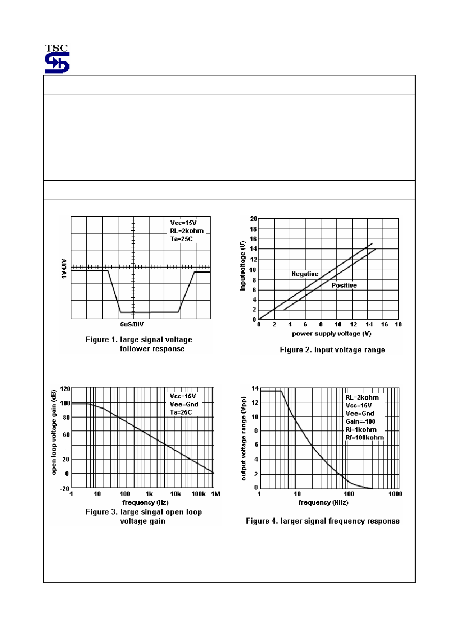
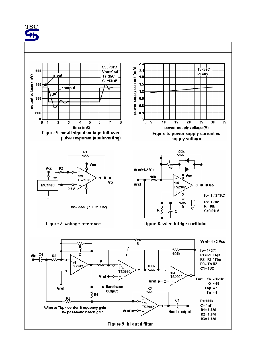
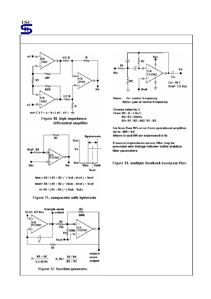
Electrical Characteristics Curve
TS2902
4-6
2005/04 rev. B
Circuit Description
TS2902
5-6
2005/04 rev. B
Circuit Description (continued)
TS2902
6-6
2005/04 rev. B
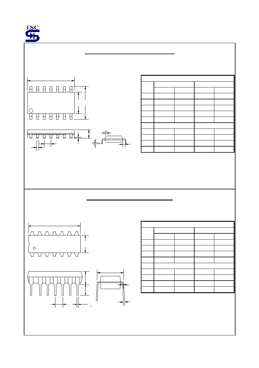
SOP-14 Mechanical Drawing
C
K
P
A
D
1
G
7
14
8
B
R
M
F
SOP-14 DIMENSION
MILLIMETERS INCHES
DIM
MIN MAX MIN MAX
A 8.55 8.75 0.337 0.344
B 3.80 4.00 0.150 0.157
C 1.35 1.75 0.054 0.068
D 0.35 0.49 0.014 0.019
F 0.40 1.25 0.016 0.049
G
1.27 (typ)
0.05 (typ)
K 0.10 0.25 0.004 0.009
M 0
o
7
o
0
o
7
o
P 5.80 6.20 0.229 0.244
R 0.25 0.50 0.010 0.019
DIP-14 Mechanical Drawing
G
K
D
C
A
1
14
B
7
8
L
M
J
DIP-14 DIMENSION
MILLIMETERS INCHES
DIM
MIN MAX MIN MAX
A 18.55 19.56 0.730 0.770
B 6.22 6.48 0.245 0.255
C 3.18 4.45 0.125 0.135
D 0.35 0.55 0.019 0.020
G
2.54 (typ)
0.10 (typ)
J 0.29 0.31 0.011 0.012
K 3.25 3.35 0.128 0.132
L 7.75 8.00 0.305 0.315
M - 10
o
- 10
o