TS2903
1-6
2005/04 rev. A
TS2903
Preliminary
Dual Voltage Comparator
Supply Voltage Range 2V to 36V
Dual Channel Comparator
General Description
The TS2903 is dual independent precision voltage comparators capable of single-supply or split-supply operation. The
specifications as low as 2.0 mV make this device an excellent ground level with single-supply operation. Input
offset-voltage selection for many applications in consumer automotive, and It is designed to permit a common mode
range-to- industrial electronics.
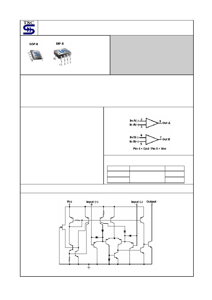
The TS2903 is offered in 8 pin SOP-8 and DIP-8 package.
Block Diagram
Features
Output voltage compatible with DTL, ECL, TTL,
MOS and CMOS Logic Levels
Low input bias current -25nA
Low input offset current �5nA
Low input offset voltage �3mV(max)
Input common mode range to ground level
Differential lnput voltage range equal to power
supply voltage
Very low current drain independent of supply
voltage - 0.4mA
Wide single-supply range 2V to 36V
Split-supply range
�1V to �18V
Ordering Information
Part No.
Operating Temp.
Package
TS2903CD
DIP-8
TS2903CS
-40 ~ +105
o
C
SOP-8
Schematic (each comparator)
Pin assignment:
1. Output
2. Input A (-)
3. Input A (+)
4. Gnd
5. Input B (+)
6. Input B (-)
7. Output B
8. Vcc
TS2903
2-6
2005/04 rev. A
Absolute Maximum Rating
Supply Voltage
Vcc
+36 or �18
V
Differential Input Voltage
V
IDR
36 V
Input Common Mode Voltage Range
Input Current (note 2)
V
ICR
Iin
-0.3 to 36
50
V
mA
Output Short Circuit to Ground
Output Sink Current (note 1)
Isc
Isink
Continuous
20
mA
Power Dissipation @ Ta=25
o
C
Derate above 25
o
C
1/Rja
570
5.7
mW
mW/
o
C
Operating Junction Temperature Range
T
J
0 ~ +125
o
C
Storage Temperature Range
T
STG
-65 ~ +150
o
C
Lead Temperature 1.6mm(1/16") from case for 10Sec.
T
LEAD
260
o
C
Electrical Characteristics
(V
CC
= 5V, T
LOW
Ta
T
HIGH
; unless otherwise specified.)
Characteristics Symbol Test
condition
Min
Typ
Max
Unit
Input Offset Voltage (note 3)
Vio
Ta =25
o
C
T
LOW
Ta
T
HIGH
--
--
2.0
9.0
7.0
15
mV
Input Offset Current
Iio
Ta =25
o
C
T
LOW
Ta
T
HIGH
--
--
�5.0
�5.0
�50
�200
nA
Input Offset Current (note 4)
I
IB
Ta =25
o
C
T
LOW
Ta
T
HIGH
--
--
25
200
250
500
nA
Input Common Mode
Voltage Range (note 5)
V
ICR
Ta =25
o
C
T
LOW
Ta
T
HIGH
0
0
--
--
V
CC
-1.5
V
CC
-2.0
V
Voltage Gain
A
VOL
R
L
15K, Vcc = 15Vdc.
Ta =25
o
C
25 200 -- V/mV
Large Signal Response
Time
--
Vin = TTL Logic Swing.
Vref = 1.4Vdc, VRL = 5Vdc.
RL 5.1K
, Ta =25
o
C
-- 300 -- nS
Response Time (note 6)
t
TLH
VRL = 5Vdc, RK = 5.1K
Ta =25
o
C
-- 1.5 -- uS
Input Differential Voltage
(note 7)
V
ID
All Vin
Gnd or V-Supply
(if used)
-- -- V
CC
V
Output Sink Current
I
SINK
Vin-
1Vdc, Vin+=0Vdc,
V
O-
1 Vdc, Ta =25
o
C
6.0 16 -- mA
Output Saturation Voltage
V
OL
Vin-
1Vdc, Vin+=0,
I
SINK
4mA, Ta =25
o
C
T
LOW
Ta
T
HIGH
--
--
--
200
400
700
mV
Output Leakage Current
I
OL
Vin-=0V, Vin+
1Vdc, P=5Vdc.
Ta =25
o
C
Vin-=0V, Vin+
1V, V
O
=30Vdc
T
LOW
Ta
T
HIGH
--
--
0.1
--
--
1000
nA
Supply Current
I
cc
R
L
=
,
Ta =25
o
C
R
L
=
,
V
CC
=30 V
--
--
0.4
--
1.0
2.5
mA
TS2903
3-6
2005/04 rev. A
Electrical Characteristics (Continues)
Note 1
.
The max. Output current may be as high as 20mA, independent of the magnitude of V
CC
, output short circuits to
V
CC
can cause excessive heating and eventual destruction.
Note 2. This magnitude of input current will only occur if the input leads are driven more negative than ground or the
negative supply voltage. This is due to the input PNP collector base junction becoming forward biased acting as
an input clamp diode. There is also a lateral PNP parasitic transistor action on the IC chip. This phenomena can
cause the output voltage of the comparators to go to the V
CC
voltage level (or ground if overdrive is large) during
the time the input is driven negative. This will not destroy the device and normal output states will recover when
the inputs become -0.3V of ground or negative supply.
Note 3. At output switch point, V
O
=1.4Vdc, R
S
=0
with V
CC
from 5Vdc to 30Vdc, and over the full input common-mode
Note 4. Due to the PNP transistor inputs, bias current will flow out of the inputs, this current is essentially constant
independent of the output state, therefore, no loading changes will exist on the input lines.
Note 5. Input common mode of either input should not be permitted to go more than 0.3V negative of ground or minus
supply. The upper limit of common mode range is V
CC
- 1.5V but either or both inputs can betaken to as high as
30volts without damage.
Note 6. Response time is specified with a 100mV step and 5.0mV of overdrive. With larger magnitudes of overdrive
faster response times are obtainable.
Note 7. The comparator will inhibit proper output state if one of the inputs is become greater than V
CC,
the other input
must remain within the common mode range. The low input state must not be less than -0.3volts of ground of
minus supply.
TS2903
4-6
2005/04 rev. A
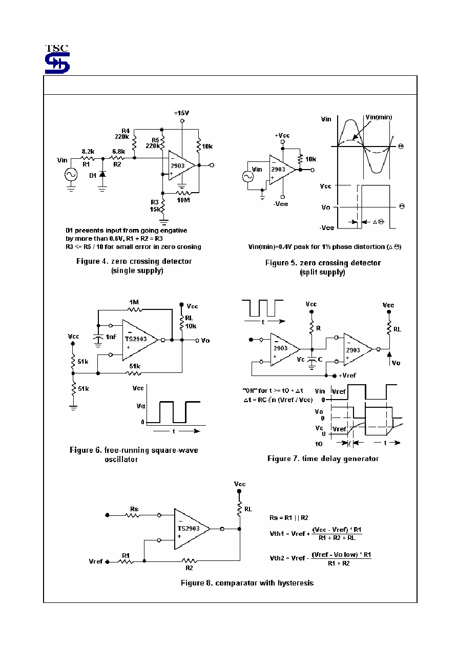
Applications Information
This dual comparator feature high gain, wide bandwidth characteristics. This gives the device oscillation tendencies if
the outputs are capacitive coupled to the inputs via stray capacitance. This oscillation manifests itself during output
transitions (V
OL
to V
OH
). To alleviate this situation input resistors<10K
should be used. The addition of positive
feedback (<10 mV) is also recommended.
It is good design practice to ground all unused pins. Differential input voltages may be larger than supply voltage
without damaging the comparator's inputs. Voltages more negative than -0.3V should not be used.
TS2903
5-6
2005/04 rev. A
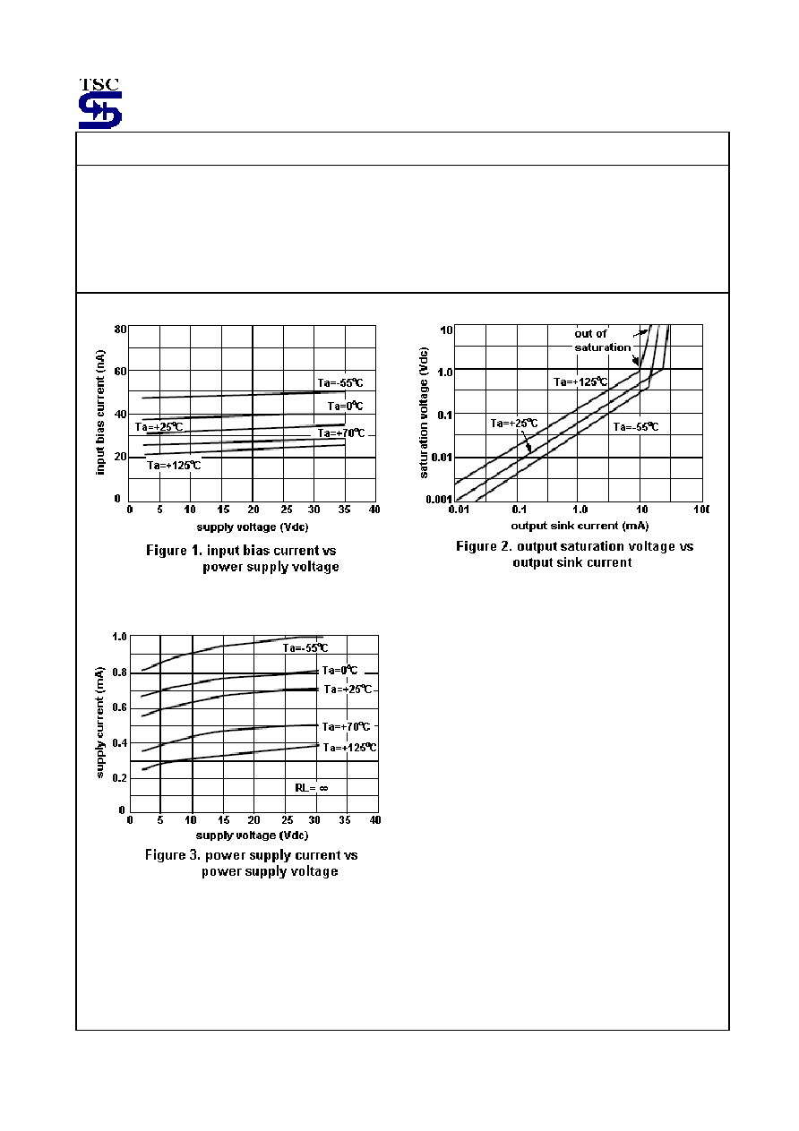
Electrical Characteristics Curve
TS2903
6-6
2005/04 rev. A
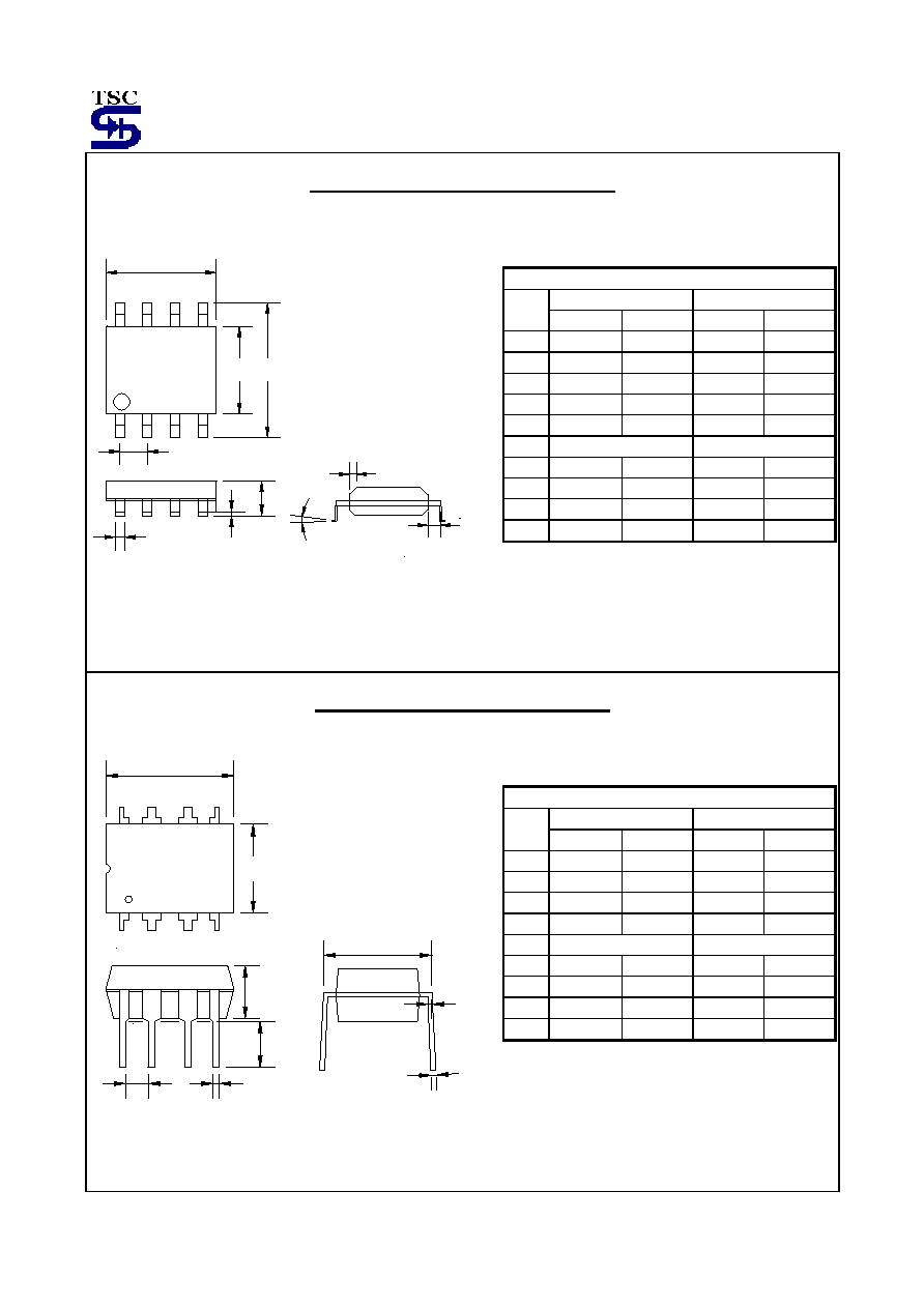
SOP-8 Mechanical Drawing
C
P
B
D
K
G
1
8
A
16
9
R
M
F
SOP-8 DIMENSION
MILLIMETERS INCHES
DIM
MIN MAX MIN MAX
A 4.80 5.00 0.189 0.196
B 3.80 4.00 0.150 0.157
C 1.35 1.75 0.054 0.068
D 0.35 0.49 0.014 0.019
F 0.40 1.25 0.016 0.049
G
1.27 (typ)
0.05 (typ)
K 0.10 0.25 0.004 0.009
M 0
o
7
o
0
o
7
o
P 5.80 6.20 0.229 0.244
R 0.25 0.50 0.010 0.019
DIP-8 Mechanical Drawing
C
K
D
G
B
A
1
8
4
5
L
M
J
SOP-8 DIMENSION
MILLIMETERS INCHES
DIM
MIN MAX MIN MAX
A 9.07 9.32 0.357 0.367
B 6.22 6.48 0.245 0.255
C 3.18 4.45 0.125 0.135
D 0.35 0.55 0.019 0.020
G
2.54 (typ)
0.10 (typ)
J 0.29 0.31 0.011 0.012
K 3.25 3.35 0.128 0.132
L 7.75 8.00 0.305 0.315
M - 10
o
- 10
o