 | –≠–ª–µ–∫—Ç—Ä–æ–Ω–Ω—ã–π –∫–æ–º–ø–æ–Ω–µ–Ω—Ç: TS29100CW | –°–∫–∞—á–∞—Ç—å:  PDF PDF  ZIP ZIP |
TS29100/1/2
1-1
2003/12 rev. A
TS29100/1/2
1.0A Ultra Low Dropout Positive Voltage Regulator
Low Dropout Voltage 0.4V typ.
Enable Input Control
Adjustable Output
Error Flag Detection
General Description
The TS29100/1/2 series are using process with a PNP pass element for high current, high accuracy and low dropout
voltage regulators. These regulator s feature 400mV(typ) dropout voltages and very low ground current, these devices
also find applications in lower current and low dropout critical systems, where their tiny dropout voltage and ground
current values are important attributes.
The TS29100/1/2 series are fully protected against over current faults, reversed input polarity, reversed lead insertion,
over temperature operation, positive and negative transient voltage spikes, logic level enable control and error flag which
signals whenever the output falls out of regulation.
On the TS29101 and TS29102, the enable pin may be tied to Vin if it is not required for enable control. This series are
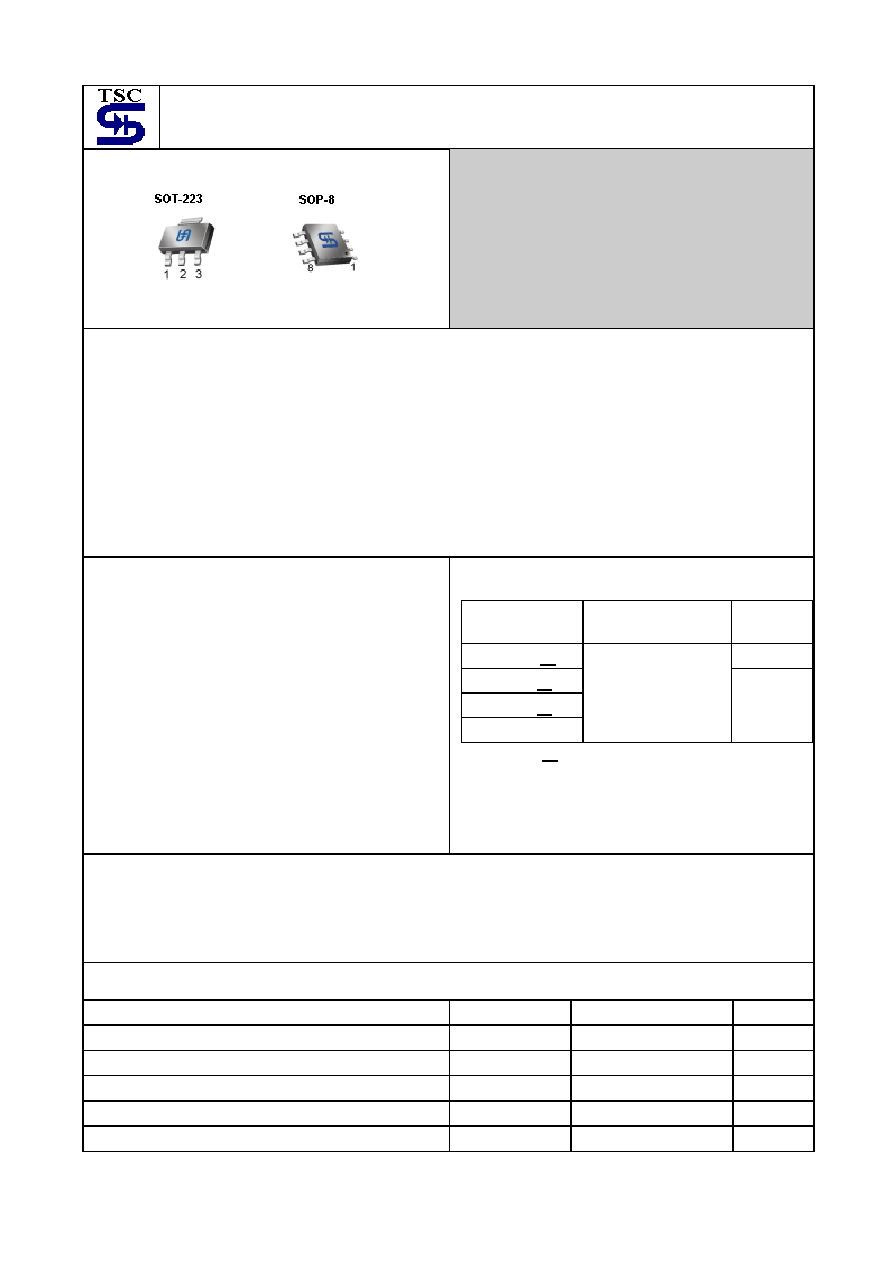
offered in 3-pin SOT-223 and 8-pin SOP pacakge.
Features
Dropout voltage typically 0.4V @Io=1.0A
Output current up to 1.0A
Low ground current
Output voltage trimmed before assembly
Extremely fast transient response
+60V Transient peak voltage
-20V Reverse peak voltage
Zero current shutdown mode
Error flag signals output out of regulation
Internal current limit
Thermal shutdown protection
Ordering Information
Note: Where
xx
denotes voltage option, available are
12V, 5.0V, 3.3V and 2.5V. Leave blank for
adjustable version. Contact factory for additional
voltage options.
Part No.
Operating Temp.
(Junction)
Package
TS29100CW
xx
SOT-223
TS29101CS
xx
TS29102CS
xx
TS29102CS
-40 ~ +125
o
C
SOP-8
Applications
Battery power equipment
Automotive electronics
High efficiency "Green" computer system
High efficiency linear power supplies
High efficiency post regulator for switching supply
Absolute Maximum Rating
(Note 1)
Input Supply Voltage (Note 2)
Vin
-20V ~ +60
V
Operation Input Voltage Vin
(operate)
26
V
Power Dissipation (Note 3)
P
D
Internally Limited
W
Operating Junction Temperature Range
T
J
-40 ~ +125
o
C
Storage Temperature Range
T
STG
-65 ~ +150
o
C
Lead Soldering Temperature (260
o
C)
5
S
TS29100/1/2
2-2
2003/12 rev. A
Electrical Characteristics
Vin = Vout + 1V, Venable= 2.4V, I
L
= 10mA, C
o
= 10uF, Adjustable versions are programmed to 5V output, Ta = 25
o
C
unless otherwise specified.
Parameter Conditions
Min
Typ
Max
Unit
Output Voltage
0.990|Vo|
1.010|Vo|
Output Voltage
10mA
I
L
1.0A,
Vo+1V
Vin 26V
0.980|Vo|
12 / 5.0
3.3/ 2.5
1.020|Vo|
V
Input Supply Voltage
--
--
26
V
Output Voltage Temperature
Coefficient
--
20
100
ppm/
o
C
Line Regulation
Vo+1V
Vin 26V
--
0.05
0.5
%
Load Regulation
10mA
I
L
1.0A
--
0.2
1.0
%
Dropout Voltage (Note 4)
I
L
=100mA
I
L
=500mA
I
L
=1.0A
--
--
--
100
200
400
200
600
mV
Quiescent Current (Note 5)
I
L
=500mA
I
L
=1.0A
--
--
4
10
--
20
mA
Short Circuit Current (Note 6)
Vout=0
--
2.0
--
A
Output Noise,
10Hz
to 100KHz, I
L
=100mA
C
L
=2.2uF
C
L
=10uF
C
L
=33uF
--
--
--
600
400
260
--
--
--
uVrms
Reference (TS29102CS)
Reference Voltage
0.980|Vo|
1.020|Vo|
Reference Voltage
10mA
I
L
1.5A,
2.3V
Vin 26V
0.970|Vo|
1.24
1.030|Vo| V
Adjust Pin Bias Current
--
40
80
nA
Reference Voltage Temperature
Coefficient
(Note
7)
-- 20 --
ppm/
o
C
Adjust Pin Bias Current
Temperature Coefficient
-- 0.1 --
nA/
o
C
Flag Output (TS29101CS)
Output Leakage Current
V
OH
=26V --
--
2
uA
Output Low Voltage
Vin=4.5V, I
OL
=250uA --
--
300
mV
Upper Threshold Voltage
(Note 8)
40
60
--
mV
Lower Threshold Voltage
(Note 8)
--
75
95
mV
Hysteresis
(Note
8)
-- 15 --
mV
Enable Input (TS29101 / TS29102)
Low (OFF)
--
--
0.8
Input Logic Voltage
High (ON)
2.4
--
--
V
Ven=26V --
--
750
Enable Pin Input Current
Ven=0.8V --
--
5
uA
Regulator Output Current
Shutdown
Ven
0.8V, Vin 26V,
Vout=0
-- 10 500
uA
TS29100/1/2
3-3
2003/12 rev. A
Thermal Performance
Condition Package
type
Typ Unit
SOT-223 15
Thermal Resistance
Junction to Ambient
SOP-8 20
o
C/W
Note 1: Absolute Maximum Rating is limits beyond which damage to the device may occur. For guaranteed
specifications and test conditions see the Electrical Characteristics.
Note 2: Maximum positive supply voltage of 60V must be limited duration (<100mS) and duty cycle (<1%).
Note 3: The maximum allowable power dissipation is a function of the maximum junction temperature, Tj, the junction to
ambient thermal resistance, ja, and the ambient temperature, Ta. Exceeding the maximum allowable power
dissipation will cause excessive die temperature, and the regulator will go into thermal shutdown. The effective
value of ja can be reduced by using a heatsink.
Note 4: Dropout voltage is defined as the input to output differential at which the output voltage drops 2% below its
nominal value measured at 1V differential.
Note 5: Ground pin current is the regulator quiescent current. The total current drawn from the source is the sum of the
ground pin current and output load current.
Note 6: Output current will decrease with increasing temperature, but it will be not dropped below 1.0A at the maximum
specified temperature.
Note 7: Thermal regulation is defined as the change in output voltage at a time T after a change in power dissipation is
applied, excluding load or line regulation effects. Specification are for a 200mA load pulse at Vin=20V (a 4W
pulse) for T=10mS
Note 8: Comparator thresholds are expressed in terms of a voltage differential at the adjust terminal below the nominal
reference voltage measured at 6V input. To express these thresholds in terms of output voltage change,
multiply by the error amplifier gain = Vout / Vref = (R1+R2) / R2. For example, at a programmed output voltage
of 5V, the error output is guaranteed to go low when the output drops by 95mV x 5V / 1.24V = 384mV.
Thresholds remain constant as a percent of Vout as Vout is varied, with the dropout warning occurring at
typically 5% below nominal, 7.7% guaranteed.
TS29100/1/2
4-4
2003/12 rev. A
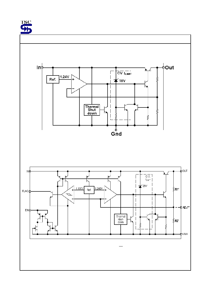
Block Diagram
TS29100
TS29101 & TS29102
* Feedback network is fixed output versions only (TS29101CS
xx
)
** Adjustable output version only (TS29102CS)
TS29100/1/2
5-5
2003/12 rev. A
Pin Assignment
Pin No.
TS29100 TS29101 TS29102
Pin
Configuration
Pin
Description
1 1
Enable
Enable (input): TTL/COMS compatible input. Logic high
is enable; logic low or open is shutdown
1 2 2
Input
Unregulated input: +26V maximum supply
2 5,6,7,8
5,6,7,8
Ground
Ground: Ground pin and TAB/heatsink are internally
connected.
3 3 3
Output Regulator
output
4
Flag
Error Flag (output): Open-collector output. Active low
indicates an output fault condition.
4
Adjust
Adjustment input: Feedback input. Connect to resistive
voltage-divider network.
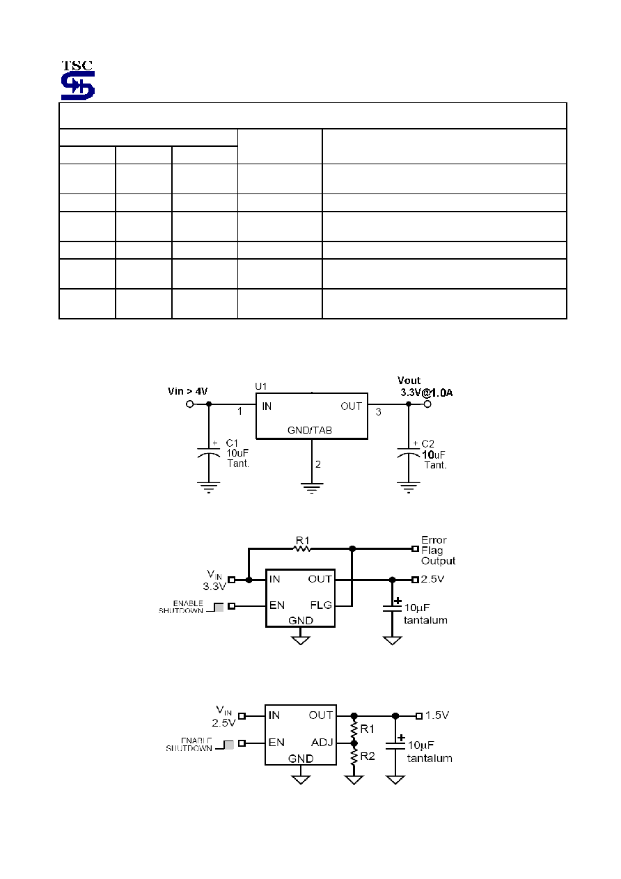
Typical Application Circuit
TS29100
TS29101
TS29102
TS29100/1/2
6-6
2003/12 rev. A
Application Information
Application Information
The TS29100/1/2 series are high performance with low
dropout voltage regulator suitable for moderate to high
current and voltage regulator application. Its
4000mA(typ) dropout voltage at full load and over
temperature makes it especially valuable in battery
power systems and as high efficiency noise filters in
post regulator applications. Unlike normal NPN
transistor design, where the base to emitter voltage
drop and collector to emitter saturation voltage limit the
minimum dropout voltage, dropout performance of the
PNP output of these devices is limited only by low Vce
saturation voltage.
The TS29100/1/2 series is fully protected from damage
due to fault conditions. Linear current limiting is
provided. Output current during overload conditions is
constant. Thermal shutdown the device when the die
temperature exceeds the maximum safe operating
temperature. Transient protection allows device survival
even when the input voltage spikes above and below
nominal. The output structure of these regulators allows
voltages in excess of the desired output voltage to be
applied without reverse current flow.
Capacitor Requirement
The TS29100/1/2 series requires an output capacitor to
maintain stability and improve transient response is
necessary. The value of this capacitor is dependent
upon the output current, lower currents allow smaller
capacitors. TS29100/1/2 series regulators are stable
with the 10uF minimum capacitor value at full load.
Where the regulator is powered from a source with high
AC impedance, a 0.1uF capacitor connected between
input and ground is recommended. The capacitor
should have good characteristics to above 250KHz. The
capacitance values will be help to improved transient
response, ripple rejection and output noise.
Minimum Load Current
The TS29100/1/2 series is specified between finite
loads. If the output current is too small leakage currents
dominate and the output voltage rises. A 10mA
minimum load current swamps any expected leakage
current across the operating temperature range.
Adjustable Regulator Design
The adjustable regulator versions (TS29102) is allow
to programming the output voltage anywhere between
1.25 and the 26V maximum operating rating of the
family.
Two resistors are used. Resistors can be quite large
up to 1M, because of the very high input impedance
and low bias current of the sense comparator, the
resistor values are calculated by:
R1 = R2 * [(Vout / 1.24) ≠ 1]
Where is Vout the desired output voltage. Above
application circuit shows component definition.
Applications with widely varying load currents may
scale the resistors to draw the minimum load current
required for proper operation.
Error Flag
TS29101 versions feature an Error Flag, which looks at
the output voltage and signals an error condition when
this voltage drops 5% below its expected value. The
error flag is an open-collector output that pulls low
under fault conditions. It may sink 10mA. Low output
voltage signifies a number of possible problems,
including an over-current fault (the device is in current
limit) and low input voltage. The flag output is
inoperative during over temperature shutdown
conditions.
Enable Input
TS29101 and TS29102 versions feature an enable
(EN) input that allows ON/OFF control of the device.
Special design allows "zero" current drain when the
device is disabled≠only microamperes of leakage
current flow. The EN input has TTL/CMOS compatible
thresholds for simple interfacing with logic, or may be
directly tied to 30V. Enabling the regulator requires
approximately 20uA of current.

TS29100/1/2
7-7
2003/12 rev. A
Application Information (continues)
Power SOP-8 Thermal Characteristics
TS29101/2 series' performance is its power SOP-8
package featuring half the thermal resistance of a
standard SOP-8 package. Lower thermal resistance
means more output current or higher input voltage for
a given package size.
Lower thermal resistance is achieved by connect the
four ground pins with the die attached pad to create a
single piece electrical and thermal conductor. This
concept have been used by MOSFET production for
years, proving very reliable and cost effective for the
user. As under:
Thermal resistance consists of two main elements, jc
(junction to case) and ca (case to ambient). Using the
power SOP-8 reduces ca, the total thermal
resistance, ja (junction to ambient) is the limiting
factor in calculating the maximum power dissipation
capability of the device. Typically, the power SOP-8
have a jc of 20
o
C/W dramatically , this is significantly
lower than the standard SOP-8 which is typically
75
o
C/W. ca is reduced because pin 5~8 can be
soldered directly to a ground plane which significantly
reduces the case to sink and sink to ambient thermal
resistance.
Power Dissipation
From under curves, the minimum area of copper
necessary for the par to operate safely can be
determined. The maximum allowable temperature rise
must be calculated to determine operation along which
curve.
TS29100/1/2
8-8
2003/12 rev. A
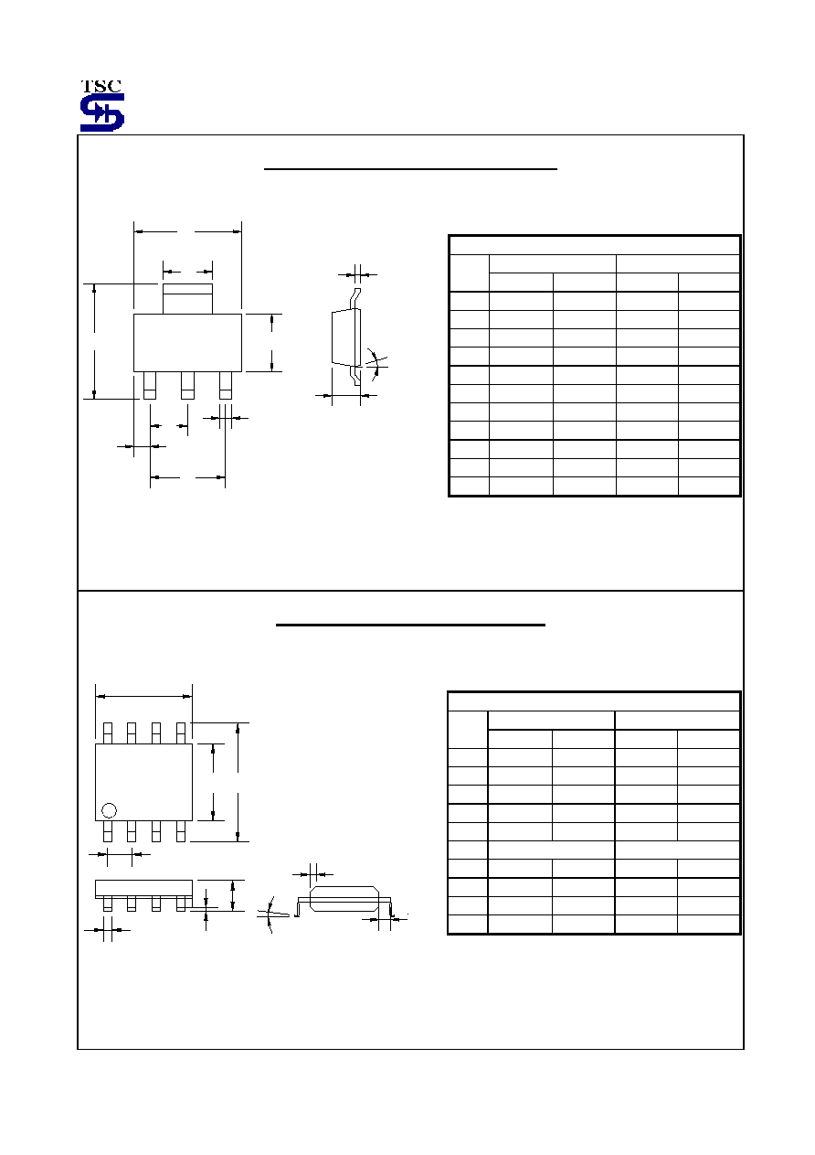
SOT-223 Mechanical Drawing
G
H
E
D
F
C
A
B
J
K
I
SOT-223 DIMENSION
MILLIMETERS INCHES
DIM
MIN MAX MIN MAX
A 6.350 6.850 0.250 0.270
B 2.900 3.100 0.114 0.122
C 3.450 3.750 0.136 0.148
D 0.595 0.635 0.023 0.025
E 4.550 4.650 0.179 0.183
F 2.250 2.350 0.088 0.093
G 0.835 1.035 0.032 0.041
H 6.700 7.300 0.263 0.287
I 0.250 0.355 0.010 0.014
J 10∞ 16∞ 10∞ 16∞
K 1.550 1.800 0.061 0.071
SOP-8 Mechanical Drawing
C
P
B
D
K
G
1
8
A
16
9
R
M
F
SOP-8 DIMENSION
MILLIMETERS INCHES
DIM
MIN MAX MIN MAX
A 4.80 5.00 0.189 0.196
B 3.80 4.00 0.150 0.157
C 1.35 1.75 0.054 0.068
D 0.35 0.49 0.014 0.019
F 0.40 1.25 0.016 0.049
G
1.27 (typ)
0.05 (typ)
K 0.10 0.25 0.004 0.009
M 0
o
7
o
0
o
7
o
P 5.80 6.20 0.229 0.244
R 0.25 0.50 0.010 0.019