TS2931 series
1-5
2004/12 rev. A
TS2931 series
100mA Ultra Low Dropout Positive Voltage Regulator
Input Voltage Range up to 30V
Output Current up to 100mA
General Description
The TS2931 voltage regulator features a very low quiescent current of 1mA or less when supplying 10mA loads. This
unique characteristic and the extremely low in-put-output differential required for proper regulation (0.2V for output
currents of 10mA) make the TS2931 the ideal regulator for standby power systems. Applications include memory standby
circuits, CMOS and other low power processor power supplies as well as systems demanding as much as 100mA of
output current.
Designed originally for automotive applications, the TS2931 and all regulated circuitry are protected from reverse battery
installations or 2 battery jumps. During line transients, such as a load dump (60V) when the input voltage to the regulator
can momentarily exceed the specified maximum operating voltage, the regulator will automatically shut down to protect
both internal circuits and the load. The TS2931 can not be harmed by temporary mirror-image insertion. Familiar regulator
features such as short circuit and thermal overload protection are also provided.
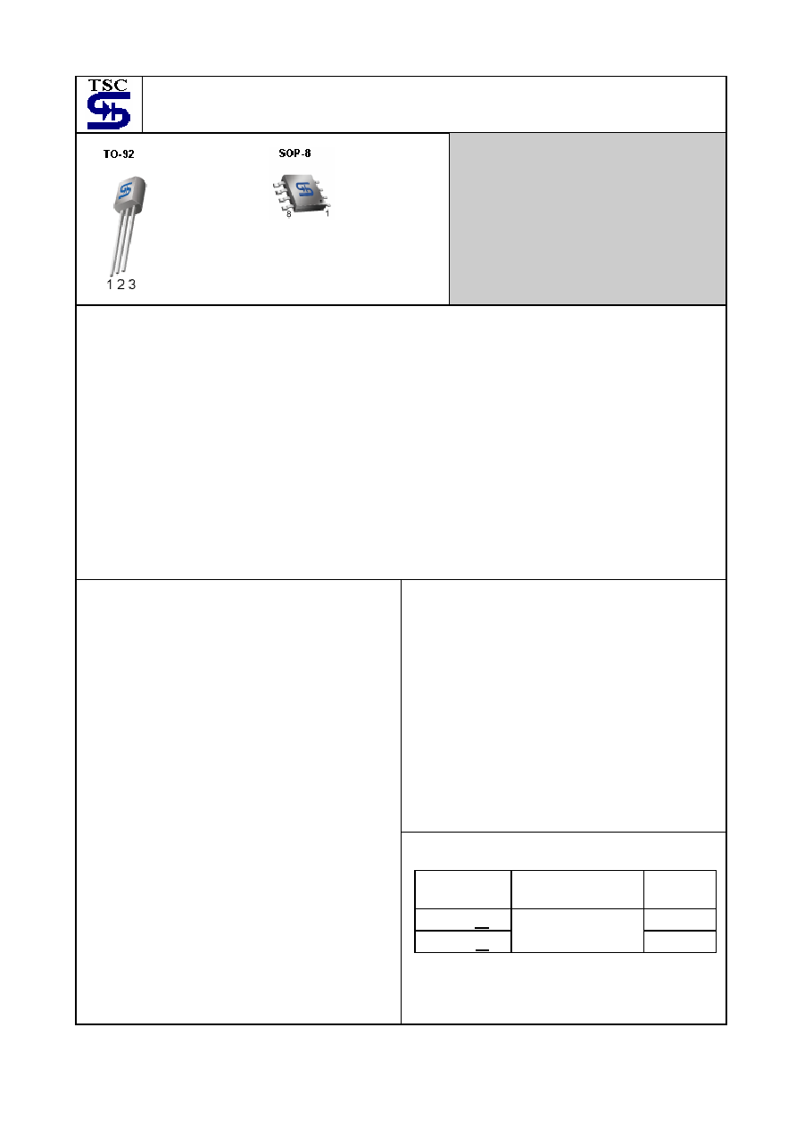
Fixed output of 5V is available in the popular TO-92 and SOT-89 package. An adjustable output version, with on/off
switch, is available in SOP-8 package.
Application
Battery powered systems
Portable
instrumentation
Avionics
Automotive
Electronics
SMPS
Post-Regulator
Voltage
Reference
Portable/Palm top / Notebook computers
Portable consumer equipment
Radio control system
Features
Very low quiescent current
Output current in excess of 100mA
Input-Output
differential less than 0.6V
Reverse battery protection
Unregulated DC input can withstand +60V positive
transients and -20V reverse battery
Short circuit protection
Internal thermal overload protection
Available as adjustable with TTL compatible switch
100% electrical burn-in in thermal limit
Available in plastic SOP-8, TO-92, SOT-89 package
Ordering Information
Note: Where xx denotes voltage option, available are
8.0V, 8.5V, 9.0V, 10V, 12V, 15V, 5.0V, 3.3V and
adjustable. Contact factory for additional voltage
options.
Part No.
Operating Temp.
(Ambient)
Package
TS2931CT
xx
TO-92
TS2931CS
xx
-20 ~ +85
o
C
SOP-8
Pin assignment
1. Output
2. Ground
3. Input
Pin assignment
1. Output
2. Gnd
3. Gnd
4. Feedback
5. Shutdown
6. Gnd
7. Gnd
8. Input
TS2931 series
2-5
2004/12 rev. A
Absolute Maximum Rating
Input Supply Voltage
Vin
- 20 ~ +35
V
Power Dissipation
Pd
Internally Limited
W
Operating Junction Temperature Range
T
J
- 55 ~ +150
o
C
Storage Temperature Range
T
STG
-65 ~ +150
o
C
Lead Temperature (Soldering 5 second)
T
STG
260
o
C
Electrical Characteristics
(V
IN
=14V,Io=100uA, T
J
=25 (Note 1), Co=100�F(unless otherwise specified)
Parameter Conditions
Min.
Typ.
Max.
Units
-20Tj 85
Full operating temperature
0.985|Vo|
0.98|Vo|
Vo
1.015|Vo|
1.02|Vo|
Output Voltage (Fix Type)
Io =100uA ~ 100mA, Tj Tj max
0.975|Vo|
--
1.025|Vo|
Input Supply Voltage
--
--
26
V
Line Regulation
13VV
IN
16V --
4
30
mV
Load Regulation
5mAIo100mA --
14
50
mV
Dropout Voltage
Io=10mA
Io=100mA
--
60
300
200
600
V
Ground Current
Io=100uA
Io=10mA
Io=100mA
--
--
--
0.1
0.9
8
0.15
1.5
12
mA
Current Linit
Vout=0
--
160
200
mA
Output Noise Voltage
10Hz-100KHz, C
OUT
=100�F --
500
--
uVRMS
Ripple Rejection Ratio
Io =10mA, fo=120Hz
60
--
--
dB
Adjustable Type Only
Vout = 3V, Io100mA, R1=27K
1.21
1.235
1.26
Reference Voltage
Full Operation Temperature 1.185
--
1.285
V
Feedback Pin Bias Current
--
20
40
nA
Feedback Pin Bias Current
Temperature Coefficient
-- -- --
nA/
Reference Voltage
Temperature Cofficient
-- 50 --
ppm/
Shutdown Input
Input Logic Voltage
Low (Regulator ON)
High (Regulator OFF)
--
2
1.3
--
0.7
--
V
Shutdown Pin Input Current
Vs=2.4V
Vs=26V
--
30
450
50
600
Regulator Output Current in Shutdown
--
3
10
uA
Note 1: Output or reference voltage temp. coefficients defined as the worst case voltage change divided by the total
temp. range.
Note 2: Regulations is measured at constant junction temperature, using pulse testing with a low duty cycle. Changes in
output voltage due to heating effects is covered under the specification for thermal regulation.
Note 3: Line regulation is tested at 125for IL=1mA, For IL=100�A and TJ=125.
Note 4: Dropout voltage is defined as the input to output differential at which the output voltage drops 2 below it's
nominal value measured at 1V differential.
Note 5: Ground pin current is the regulator quiescent current. The total current drawn form the source is the sum of the
ground pin current and output load current.
Note 6: Thermal regulation is the change in output voltage at a time T after a change in power dissipation, excluding load
or line regulation effects. Specifications are for a 50mA load pulse (1.25W) for T=10ms.
Note 7: Vref Vout (Vin-1V), 2.3VVin26V, 100�AIL100mA, TJTJMAX
Note 8: Vshutdown 2V, Vin26V, Vout=0V
TS2931 series
3-5
2004/12 rev. A
Application Hints
One of the distinguishing factors of the TS2931 series regulators is the requirement of an output capacitor for device
stability. The value required varies greatly depending upon the application circuit and other factors. Thus some
comments on the characteristics of both capacitors and the regulator are in order.
High frequency characteristics of electrolytic capacitors depend greatly on the type and even the manufacturer. As a
result, a value of capacitance that works well with the TS2931 for one brand or type may not necessary be sufficient
with an electrolytic of different origin. Sometimes actual bench testing, as described later, will be the only means to
determine the proper capacitor and value. Experience has shown that, as a rule of thumb, the more expensive and
higher quality electrolytic generally allows a smaller value for regulator stability. As an example, while a high-quality
100 F aluminum electrolytic covers all general application circuits, similar stability can be obtained with a tantalum
electrolytic of only 47uF. This factor of two can generally be applied to any special application circuit also.
Another critical characteristic of electrolytic is their performance over temperature. While the TS2931 is designed to
operate to -20 , the same is not always true with all electrolytic
(hot is generally not a problem). The electrolyte in
many aluminum types will freeze around -250 ,
reducing their effective value to zero. Since the capacitance is needed
for regulator stability, the natural result is oscillation (and lots of it) at the regulator output. For all application circuits
where cold operation is necessary, the output capacitor must be rated to operate at the minimum temperature. By
coincidence, worst-case stability for the TS2931 also occurs at minimum temperatures. As a result, in applications
where the regulator junction temperature will never be less than 25 , the output capacitor can be reduced
approximately by a factor of two over the value needed for the entire temperature range. To continue our example with
the tantalum electrolytic, a value of only 22uF would probably thus suffice. For high-quality aluminum, 47uF would be
adequate in such an application.
Another regulator characteristic that is noteworthy is that stability decreases with higher output currents. This sensible
fact has important connotations. In many applications, the TS2931 is operated at only a few milliamps of output current
or less. In such a circuit, the output capacitor can be further reduced in value. As a rough estimation, a circuit that is
required to deliver a maximum of 10mA of output current from the regulator would need an output capacitor of only half
the value compared to the same regulator required to deliver the full output current of 100mA. If the example of the
tantalum capacitor in the circuit rated at 25 junction temperature and above were continued to include a maximum
of
10mA of output current, then the 22uF output capacitor could be reduced to only 10uF.
In the case of the TS2931CS adjustable regulator in SOP-8 package, the minimum value of output capacitance is a
function of the output voltage. As a general rule, the value decreases with higher output voltages, since internal loop
gain is reduced.
At this point, the procedure for bench testing the minimum value of an output capacitor in a special application circuit
should be clear. Since worst-case occurs at minimum operating temperatures and maximum operating currents, the
entire circuit, including the electrolytic, should be cooled to the minimum temperature. The input voltage to the regulator
should be maintained at 0.6V above the output to keep internal power dissipation and die heating to a minimum.
Worst-case occurs just after input power is applied and before the die has had a chance to heat up. Once the minimum
value of capacitance has been found for the brand and type of electrolytic in question, the value should be doubled for
actual use to account for production variations both in the capacitor and the regulator. (All the values in this section and
the remainder of the data sheet were determined in this fashion.)
Definition of Terms
Dropout Voltage:
The input-output voltage differential at which the circuit ceases to regulate against further reduction
in input voltage. Measured when the output voltage has dropped 100 mV from the nominal value
obtained at 14V input, dropout voltage is dependent upon load current and junction temperature.
Input Voltage:
The DC voltage applied to the input terminals with respect to ground.
Input-Output Differential:
The voltage difference between the unregulated input voltage and the regulated output
voltage for which the regulator will operate.
Line Regulation:
The change in output voltage for a change input voltage. The measurement is made under
conditions of low dissipation or by using pulse techniques such that the average chip temperature
is not significantly affected.
Load Regulation:
The change in output voltage for a change in load current at constant chip temperature.
Output Noise Voltage:
The rms AC voltage at the output, with constant load and no input ripple, measured over a
specified frequency range.
Quiescent Current:
That part of the positive input current that does not contribute to the positive load current. The
regulator ground lead current.
Ripple Rejection:
The ratio of the peak-to-peak input ripple voltage to the peak-to-peak output ripple voltage.
TS2931 series
4-5
2004/12 rev. A
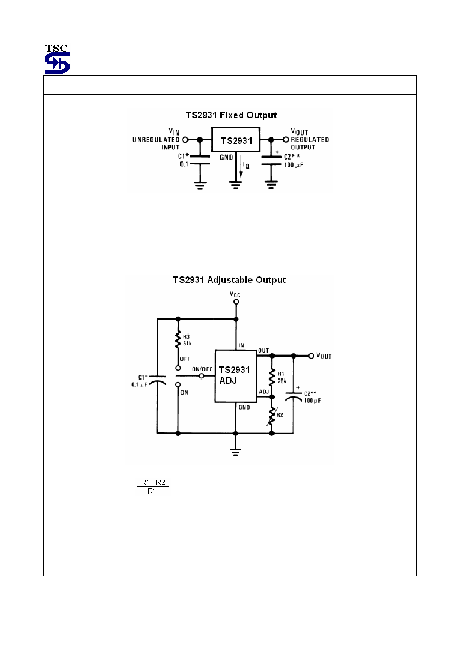
Typical Application Circuit
*Required if regulator is located far from power supply filter.
**C2 must be at least 100uF to maintain stability. May be increased without bound to maintain regulation during
transients. Locate as close as possible to the regulator. This capacitor must be rated over the same operating
temperature range as the regulator. The equivalent series resistance (ESR) of this capacitor is critical; see curve.
V
OUT
= Reference Voltage x
Note:
Using 27K for R1 will automatically compensate for errors in V
OUT
due to the input bias current of the ADJ pin
(approximately 1uA)
TS2931 series
5-5
2004/12 rev. A
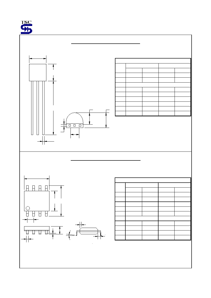
TO-92 Mechanical Drawing
C
D
A
B
H
E
F
G
TO-92 DIMENSION
MILLIMETERS INCHES
DIM
MIN MAX MIN MAX
A 4.30 4.70 0.169 0.185
B 4.30 4.70 0.169 0.185
C
14.30(typ)
0.563(typ)
D 0.43 0.49 0.017 0.019
E 2.19 2.81 0.086 0.111
F 3.30 3.70 0.130 0.146
G 2.42 2.66 0.095 0.105
H 0.37 0.43 0.015 0.017
SOP-8 Mechanical Drawing
C
P
B
D
K
G
1
8
A
16
9
R
M
F
SOP-8 DIMENSION
MILLIMETERS INCHES
DIM
MIN MAX MIN MAX
A 4.80 5.00 0.189 0.196
B 3.80 4.00 0.150 0.157
C 1.35 1.75 0.054 0.068
D 0.35 0.49 0.014 0.019
F 0.40 1.25 0.016 0.049
G
1.27 (typ)
0.05 (typ)
K 0.10 0.25 0.004 0.009
M 0
o
7
o
0
o
7
o
P 5.80 6.20 0.229 0.244
R 0.25 0.50 0.010 0.019