TS2938/A
1-5
2004/09 rev. A
TS2938/A
500mA Ultra Low Dropout Fixed Voltage Regulator with Inhibit
Low Dropout Voltage 0.6V max.
Logic Inhibit Control
General Description
T
he TS2938/A series of fixed-voltage monolithic micro-power voltage regulators is designed for a wide range of
applications. This device excellent choice of use in battery-power application. Furthermore, the quiescent current
increases on slightly at dropout, which prolongs battery life.
This series of fixed-voltage regulators features very low ground current (100uA Typ.), very low drop output voltage (Typ.
60mV at light load and 600mV at 500mA) and output inhibit control. This includes a tight initial tolerance of 1% (TS2938A)
and 2% (TS2938), extremely good line regulation of 0.05% typ., and very low output temperature coefficient.
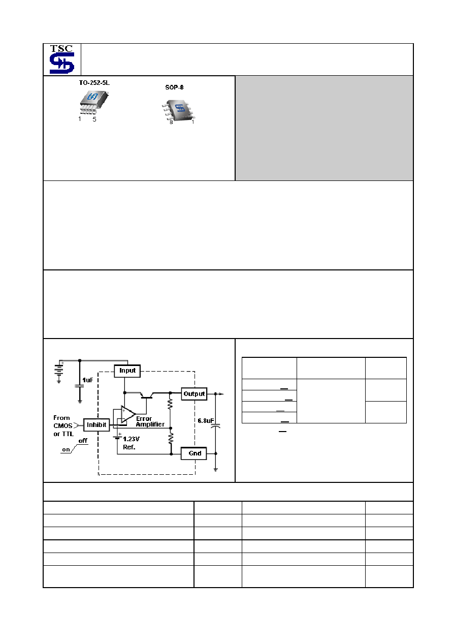
This series is offered in 5-pin of TO-252-5L and 8-pin SOP-8 package.
Features
Dropout voltage typically 0.5V @Io=500mA
Output current up to 500mA
Logic control electronic shutdown
Output voltage trimmed before assembly
-18V Reverse peak voltage
+30V Input over voltage protection
+60V Transient peak voltage
Low quiescent current 100uA typ. (ON mode),
Internal current limit
Thermal shutdown protection
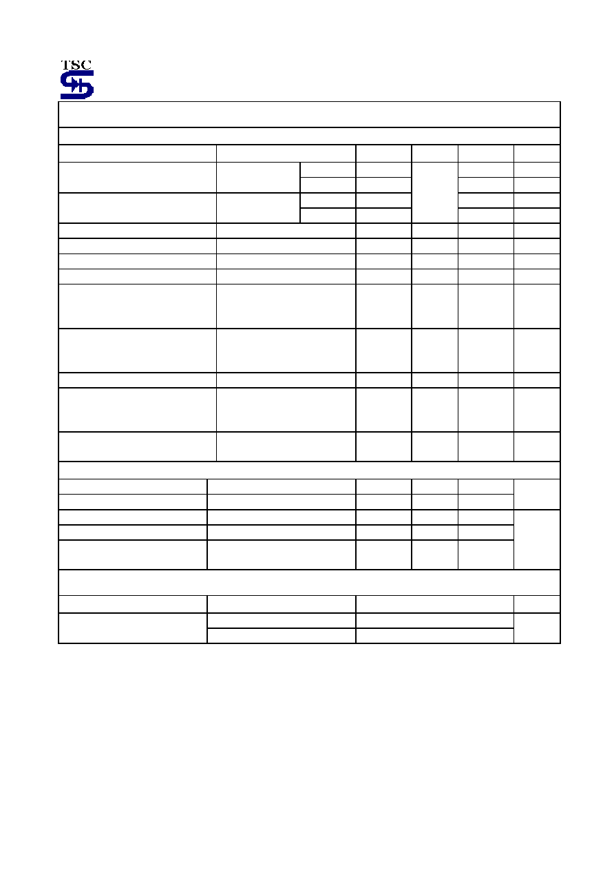
Block Diagram
Ordering Information
Part No.
Operation Temp.
(Ambient)
Package
TS2938CP5
xx
TS2938ACP5
xx
TO-252-5L
TS2938CS
xx
TS2938ACS
xx
-20 ~ +85
o
C
SOP-8
Note: Where
xx
denotes voltage option, available are
8.0V, 5.0V, 3.3V and 2.5V. Contact factory for
additional voltage options.
Absolute Maximum Rating
(Note 1)
Input Supply Voltage (Note 2)
Vin
-18 ~ +60
V
Operation Input Supply Voltage Vin
(operate)
26
V
Power Dissipation (Note 3)
P
D
Internally Limited
W
Operating Junction Temperature Range
T
J
-40 ~ +125
o
C
Storage Temperature Range
T
STG
-65 ~ +150
o
C
Lead Soldering Temperature (260
o
C)
TO-252 / SOP-8 Package
5
S
Pin assignment:
1. Output 8. Input
2. Gnd
7. Gnd
3. Gnd
6. Gnd
4. N/C
5. Inhibit
Pin assignment:
1. Input
2. Inhibit
3. Gnd
4. N/C
5. Output
TS2938/A
2-5
2004/09 rev. A
Electrical Characteristics
Vin = Vout + 1V, I
L
= 5mA, C
o
= 6.8uF, Ta = 25
o
C, Vinhibit = 0V, unless otherwise specified.
Parameter Conditions
Min
Typ
Max
Unit
TS2938A 0.990|Vo|
1.010|Vo| v
Output Voltage
Ta = 25
o
C
TS2938 0.980|Vo|
1.020|Vo| V
TS2938A 0.980|Vo|
1.020|Vo|
Output Voltage
Ta = -25 ~ 85
o
C
TS2938 0.960|Vo|
8.0 / 5.0
3.3 / 2.5
1.040|Vo| V
Input Supply Voltage
--
--
26
V
Output Voltage Temp. Coefficient
--
50
150
ppm/
o
C
Line Regulation
Vo+1V
Vin 26V
--
0.05
0.5
%
Load Regulation
5mA
I
L
500mA
--
0.2
1.0
%
Dropout Voltage (Note 4)
I
L
=100mA
I
L
=300mA
I
L
=500mA
--
--
--
100
300
500
200
400
600
mV
Quiescent Current (Note 5)
I
L
=100uA
I
L
=300mA
I
L
=500mA
--
--
--
100
12
25
200
20
50
uA
mA
Short Circuit Current (Note
6) Vout=0
-- 0.9 1.3 A
Output Noise,
10Hz
to 100KHz, I
L
=10mA
C
L
=2.2uF
C
L
=3.3uF
C
L
=33uF
--
--
--
500
350
120
--
--
--
uVrms
Ripple Rejection Ratio
Io=350mA, f=120Hz,
Co=100uF, Vin=Vo+3V+2Vpp
60 -- -- dB
Shutdown Input
Input Logic Voltage
Low (Regulator ON)
--
1.3
0.7
High (Regulator OFF)
2.0
--
--
V
Shutdown Pin Input Current
Vinhibit = 2.4V
--
30
50
Vinhibit = 26V
--
450
600
Regulator Output Current in
Shutdown
Vinhibit
2V, Vin 26V,
Vout = 0V
-- -- 200
uA
Thermal Performance
Condition Package
type
Typ
Unit
TO-252 150
Thermal Resistance
Junction to Ambient
SOP-8 170
o
C/W
Note 1: Absolute Maximum Rating is limits beyond which damage to the device may occur. For guaranteed Specifications
and test conditions see the Electrical Characteristics.
Note 2: Maximum positive supply voltage of 60V must be limited duration (<100mS) and duty cycle (<1%).
Note 3: The maximum allowable power dissipation is a function of the maximum junction temperature, Tj, the junction to
ambient thermal resistance, ja, and the ambient temperature, Ta. Exceeding the maximum allowable power
dissipation will cause excessive die temperature, and the regulator will go into thermal shutdown. The effective
value of ja can be reduced by using a heatsink.
Note 4: Dropout voltage is defined as the input to output differential at which the output voltage drops 2% below its
nominal value measured at 1V differential.
Note 5: Ground pin current is the regulator quiescent current. The total current drawn from the source is the sum of the
ground pin current and output load current.
Note 6: Output current will decrease with increasing temperature, but it will be not dropped below 500mA at the maximum
specified temperature.
TS2938/A
3-5
2004/09 rev. A
Application Information
The TS2938/A series is a high performance with low
dropout voltage regulator suitable for moderate to high
current and voltage regulator application. Its 500Mv (typ)
dropout voltage at full load and over temperature makes it
especially valuable in battery power systems and as high
efficiency noise filters in post regulator applications. Unlike
normal NPN transistor design, where the base to emitter
voltage drop and collector to emitter saturation voltage
limit the minimum dropout voltage, dropout performance
of the PNP output of these devices is limited only by low
Vce saturation voltage.
The TS2938/A series is fully protected from damage due
to fault conditions. Linear current limiting is provided.
Output current during overload conditions is constant.
Thermal shutdown the device when the die temperature
exceeds the maximum safe operating temperature.
Transient protection allows device survival even when the
input voltage spikes above and below nominal. The output
structure of these regulators allows voltages in excess of
the desired output voltage to be applied without reverse
current flow.
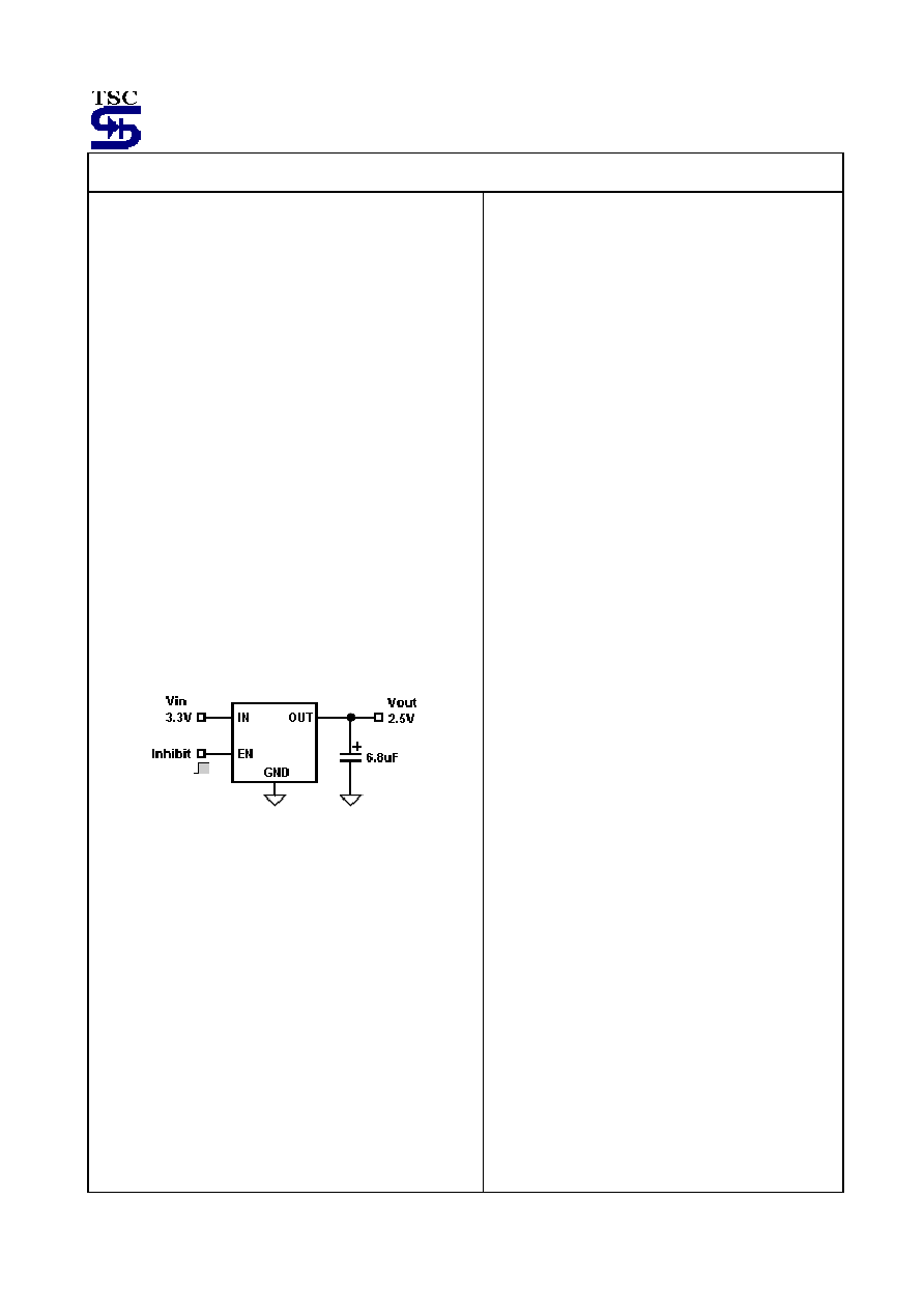
Typical Application Circuit
Output Capacitor
The TS2938/A series requires an output capacitor to
maintain stability and improve transient response. Proper
capacitor selection is important to ensure proper
operation. The output capacitor selection is dependent
upon the ESR of the output capacitor the maintain
stability. When the output capacitor is 6.8uF or greater,
the output capacitor should have an ESR less than 2 ohm.
This will improve transient response as well as promoted
stability. Ultra low ESR capacitors (<100mohm), such as
ceramic chip capacitors may promote instability. These
very low ESR levels may cause an oscillation and/or
under damped transient response. A low ESR solid
tantalum capacitor works extremely well and provide
good transient response and stability over
temperature. Aluminum electrolytic can also be
used, as long as the ESR of the capacitor is <2ohm.
The value of the output capacitor can be increased
without limit. Higher capacitance values help to
improved transient response and ripple rejection and
reduce output noise.
Minimum Load Current
The TS2938/A series is specified between finite
loads. If the output current is too small leakage
currents dominate and the output voltage rises. A
5mA minimum load current is necessary for proper
regulation.
Input Capacitor
An input capacitor of 1uF or greater is
recommended when the device is more that 4
inches away from the bulk AC supply capacitance or
when the supply is a battery. Small and surface
mount ceramic chip capacitors can be used for
bypassing. Larger values will help to improve ripple
rejection by bypassing the input to the regulator,
further improving the integrity of the output voltage.
Thermal Characteristics
A heatsink may be required depending on the
maximum power dissipation and maximum ambient
temperature of the application. Under all possible
operating conditions, the junction temperature must
be within the range specified under absolute
maximum ratings. To determine if the heatsink is
required, the power dissipated by the regulator, P
D
must be calculated.
The below formula shows the voltages and currents
for calculating the P
D
in the regulator:
Iin = I
L
/ I
G
P
D
= (Vin-Vout) * I
L
+ (Vin) * I
G
Ex. P
D
= (3.3V-2.5V) * 0.5A + 3.3V * 11mA
= 400mW + 36mW
= 436mW
Remark: I
L
is output load current,
I
G
is ground current.
Vin is input voltage
Vout is output voltage
TS2938/A
4-5
2004/09 rev. A
Application Information (continued)
The next parameter which must be calculated the
maximum allowable temperature rise.
T
R
(max) is calculated by the using to formula:
T
R
(max) = T
J
(max) � T
A
(max)
Where: T
J
(max) is the maximum allowable junction
temperature, which is 125
o
C for commercial
grade parts.T
A
(max) is the maximum ambient
temperature which will be encountered in the
application.
Using the calculated values for T
R
(max) and P
D
, the
maximum allowable value for the junction to ambient
thermal resistance,
ja
, can now be found:
ja
= T
R
(max) / P
D
Inhibit Input
TS2938/A feature an active-low (Inhibit) input that
allows ON/OFF control of the regulator. The Inhibit
input has TTL/CMOS compatible thresholds for simple
interfacing with logic interfacing. Inhibit should be
directly tied to Ground or keep open (not connected).
IMPORTANT:
if the maximum allowable value for is found to be 60
o
C/W for the TO-220 package, 80
o
C/W for the
TO-263 package, 150
o
C/W for the TO-252 package,
or 170
o
C/W for the SOT-223 package, no heatsink is
needed since the package alone will dissipate enough
heat to satisfy these requirements. If the calculated
value for
ja
falls below these limits, a heatsink is
required.
TS2938/A
5-5
2004/09 rev. A
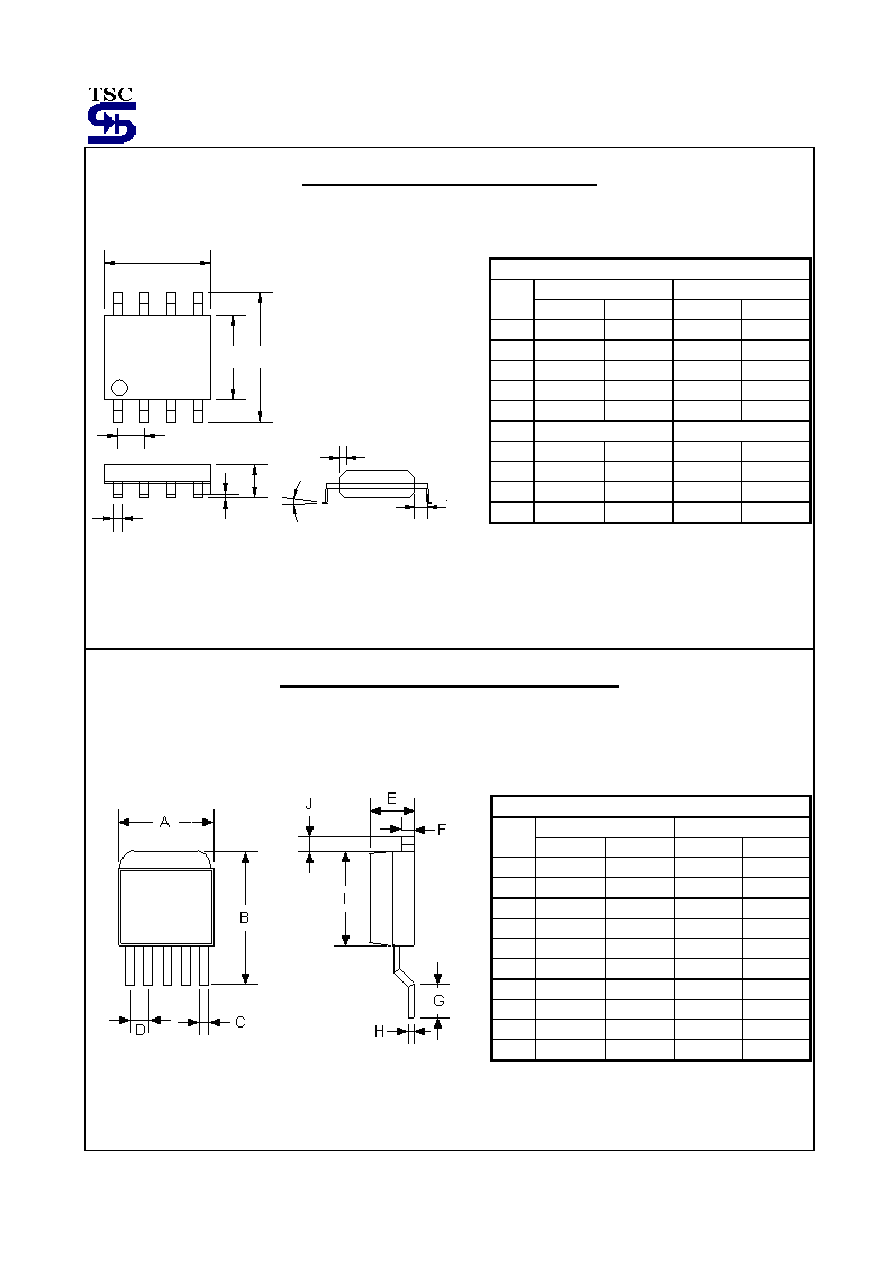
SOP-8 Mechanical Drawing
C
P
B
D
K
G
1
8
A
16
9
R
M
F
SOP-8 DIMENSION
MILLIMETERS INCHES
DIM
MIN MAX MIN MAX
A 4.80 5.00 0.189 0.196
B 3.80 4.00 0.150 0.157
C 1.35 1.75 0.054 0.068
D 0.35 0.49 0.014 0.019
F 0.40 1.25 0.016 0.049
G
1.27 (typ)
0.05 (typ)
K 0.10 0.25 0.004 0.009
M 0
o
7
o
0
o
7
o
P 5.80 6.20 0.229 0.244
R 0.25 0.50 0.010 0.019
TO-252-5L Mechanical Drawing
TO-252-5L DIMENSION
MILLIMETERS INCHES
DIM
MIN MAX MIN MAX
A 6.350 6.730 0.2509 0.265
B 9.250 10.400 0.364 0.409
C 0.460 0.640 0.018 0.025
D 2.560 2.670 0.101 0.105
E 2.190 2.380 0.086 0.094
F 0.460 0.570 0.018 0.022
G 1.400 1.780 0.055 0.070
H 0.460 0.570 0.018 0.022
I 5.340 5.550 0.210 0.219
J 1.520 2.030 0.060 0.080