TS2950-51 series
1-6
2003/12 rev. B
TS2950/TS2951 series
150mA Ultra Low Dropout Positive Voltage Regulator
Input Voltage Range up to 30V
Output Current up to 150mA
Low Drop Out Voltage 0.4V
General Description
The TS2950/A & TS951/A are low power voltage regulators. These devices are excellent choice for use in
battery-powered applications such as cordless telephone, radio control systems, and portable computers.
The TS2950/A & TS2951/A is features very low quiescent current (75uA Typ.) and very low drop output voltage (Typ.
40uV at light load and 380 mV at 100 mA). This includes a tight initial tolerance of 0.5% typ.(A version), extremely good
load and line regulation 0.05% typ. and very low output temperature coefficient, making the TS2950/A & TS2951/A useful
as a low-power voltage reference.
TS2951/A have other key additional feature of unregulated input voltage transient of -20V below ground (reverse battery).
The error flag output feature is used as power-on reset for warn of a low output voltage, due to following batteries on
input. The logic-compatible shutdown input which enable the regulator to be switched on/off. The regulator output voltage
may be pin-strapped for a 5.0, 3.3 & 3V of programmed from 1.24V to 29V with external pair of resistors. Using of as
design, processing and testing techniques make TS2950/A & TS951/A superior over similar products.
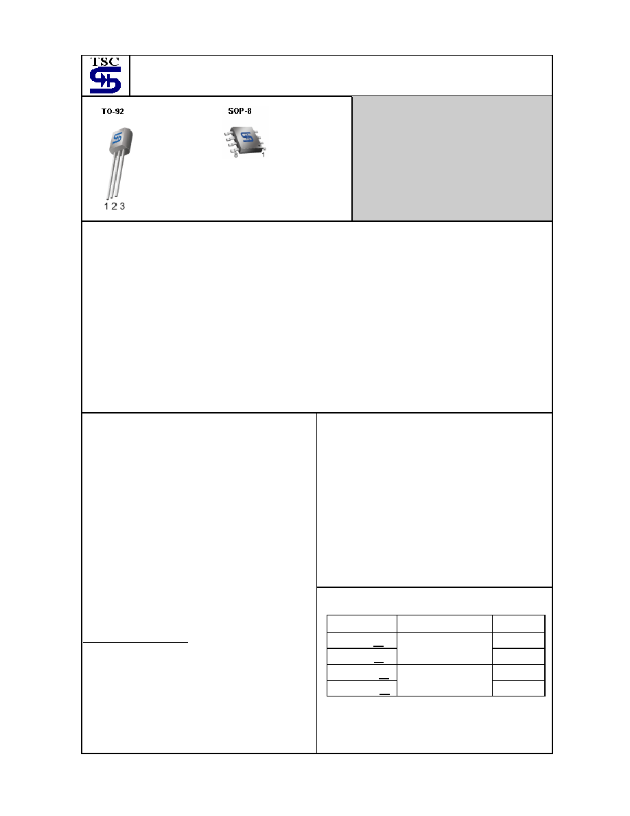
The TS2950/A is offered in 3-pin TO-92 package, The TS2951/A is available in 8-pin plastic SOP-8 package.
Application
Battery powered systems
Portable
instrumentation
Avionics
Automotive
Electronics
SMPS
Post-Regulator
Voltage
Reference
Portable/Palm top / Notebook computers
Portable
consumer
equipment
Radio control system
Features
Output voltage available in 5V, 3.3V & 3V
Extremely low quiescent current
Low
dropout
voltage
Extremely tight load and line regulation
Very low temperature coefficient
Need only 1uF for stability
Unregulated DC input can withstand -20V reverse
battery and +60V positive transients
Use as Regulator or Reference
Stable with low-ESR output capacitors
Current and thermal limiting
Direct replacement for LP2950 & LP2951 sockets
TS2951 VERSIONS ONLY
Error Flag warns of output dropout
Logic-Controlled
electronic
shutdown
Additional voltage tap
Output voltage sense
Output programmable from 1.24 to 29V
Ordering Information
Note: Where xx denotes voltage option, available are
5.0V, 3.3V and 3V. Contact factory for additional
voltage options.
Part No.
Operating Temp. Package
TS2950CT-
xx
TO-92
TS2951CS-
xx
-40 ~ +85
o
C
SOP-8
TS2950ACT-
xx
TO-92
TS2951ACS-
xx
-20 ~ +85
o
C
SOP-8
Pin assignment
TO-92
1. Output
2. Ground
3. Input
Pin assignment
SOP-8
1. Output
2. Sense
3. Shutdown
4. Ground
5. Error
6. Voltage tap
7. Feedback
8. Input
TS2950-51 series
2-6
2003/12 rev. B
Absolute Maximum Rating
Input Supply Voltage
Vin
- 0.3 ~ +30
V
Feedback Input Voltage
Vfeedback
- 1.5 ~ +30
V
Shutdown Input Voltage
Vshutdown
- 0.3 ~ +30
V
Error Comparator Output Voltage
Verror
- 0.3 ~ +30
V
Power Dissipation
Pd
Internally Limited
W
TS2950/2951
- 40 ~ +125
Operating Junction Temperature
Range
TS2950A/2951A
T
J
- 20 ~ +125
o
C
Storage Temperature Range
T
STG
-65 ~ +150
o
C
Lead Temperature (Soldering 5 second)
T
STG
260
o
C
TS2950/A & TS2951/A Electrical Characteristics
(Vin=15V, Ta=25
o
C unless otherwise specified.)
Parameter Test
Conditions
(note 2)
Min
Typ
Max
Unit
TS2950/TS2951 |0.990|
|1.010|
Tj= 25
o
C
TS2950A/TS2951A |0.995|
|1.005|
TS2950/TS2951 |0.980|
|1.020|
Full Operating temp
TS2950A/TS2951A |0.988|
|1.012|
TS2950/TS2951 |0.975|
|1.025|
Output Voltage
100uA
I
L
100mA
Tj
Tj(max)
TS2950A/TS2951A |0.985|
5.0
3.3
3.0
|1.015|
V
TS2950/TS2951 --
50
150
Output Voltage Temperature
Coefficient
(Note 1)
TS2950A/TS2951A -- 20 100
ppm/
o
C
Line Regulation (Note 3)
6V
Vin 30V (Note 4)
--
0.04
0.2
%
Load Regulation (Note 3)
100uA
I
L
100mA --
0.1
0.3
%
Dropout Voltage (Note 5)
I
L
=100uA
I
L
=100mA
-- 50
380
80
450
mV
mV
Ground Current
I
L
=100uA
I
L
=100mA
-- 75
8
120
12
uA
mA
Dropout Ground Current
Vin= 4.5V, I
L
= 100uA
--
110
170
uA
Current Limit
Vout= 0
--
160
200
mA
Thermal Regulation
--
0.05
0.2
%W
Output Noise, 10Hz
to 100KHz
Bypass=0.01uF
(pins 7 to 1 TS2951/A)
C
L
= 1uF
C
L
= 200uF
C
L
= 3.3uF
-- 430
160
100
-- uV/
rms
8-Pin TS2951/A Versions only
TS2951 1.21 1.27
Reference Voltage
TS2951A 1.22 1.26
V
TS2951 1.185
1.285
Reference Voltage
(Note6)
TS2951A 1.19
1.235
1.27
V
TS2950-51 series
3-6
2003/12 rev. B
TS2951/A Electrical Characteristics
(continues)
(Vin= 15V, Ta= 25
o
C unless otherwise specified.)
Parameter Test
Conditions
(note 2)
Min
Typ
Max
Unit
Feedback Pin Bias Current
--
20
40
nA
Reference Voltage Temperature
Coefficient
(Note 7)
-- 20 --
ppm/
o
C
Feedback Pin Bias Current
Temperature Coefficient
-- 0.1 --
nA/
o
C
Error Comparator
Output Leakage Current
V
OH
= 30V
--
0.01
1
uA
Output Low Voltage
Vin= 4.5V, I
OL
= 400uA
--
150
250
mV
Upper Threshold Voltage
(Note 8)
40
60
--
mV
Power Threshold Voltage
(Note 8)
--
75
95
mV
Hysteresis
(Note
8)
-- 15 -- mV
Shutdown Input
Output Logic Voltage
Low (Regulator ON)
High(Regulator OFF)
--
2.0
1.3
1.3
0.7
--
V
Shut down Pin Current
Vs = 2.4V
Vs = 30V
-- 30
450
50
600
uA
Regulator Output Current in
Shutdown
(Note 9)
--
3
10
uA
Note 1: Output voltage temperature coefficients defined as the worst case voltage change divided by the total
temperature range.
Note 2: Unless otherwise specified all limits guaranteed for T
j
= 25
o
C, Vin= 6V, I
L
= 100uA and C
L
= 100uF. Additional
conditions for the 8-pin versions are feedback tied to 5V, 3.3V & 3V tap output Sense (Vout = 5V, 3.3V & 3V) and
Vshutdown
0.8V.
Note 3: Regulation is measured at constant junction temperature, using pulse testing with a low duty cycle. Changes in
output voltage due to heating effects are covered under the specification for thermal regulation.
Note 4: Line regulation for the TS2951 is tested at 85
o
C for I
L
= 1mA.For I
L
= 100uA and Tj= 125
o
C, line regulation is
guaranteed by design to 0.2%.
Note 5: Dropout Voltage is defined as the input to output differential at which the output voltage drops 100mV below its
nominal value measured at 1V differential at very low value of programmed output voltage, the minimum input
supply voltage of 2V (2.3V over temperature) must be taken in to account.
Note 6: Vref
Vout (Vin-1V), 2.3 Vin 30V, 100uA I
L
100mA, Tj Tj(max)
.
Note 7: reference voltage temperature coefficient is defined as the worst case voltage change divided by the total
temperature range.
Note 8: Comparator thresholds are expressed in terms of a voltage differential at the feedback terminal below the
nominal reference voltage measured at 6V input. To express these thresholds in terms of output voltage change,
multiply by the error amplifier gain= Vout / Vref = (R1+R2) / R2. For example, at a programmed output voltage of
5V, the Error output is guaranteed to go low when the output drops by 95 mV X 5V / 1.250 = 384mV. Thresholds
remain constant as a percent of Vout as Vout is varied with the dropout warning occurring at typically 5% below
nominal, 7.5% guaranteed.
TS2950-51 series
4-6
2003/12 rev. B
Application Hints
External Capacitors
For the stability of the TS2950/A & TS2951/A is requires
a 1.0uF(0.22uF is recommended for 3.0V & 3.3V) or
greater capacitor between output and ground. Oscillation
could occur without this capacitor. The tantalum or
aluminum electrolytic works fine; could use the film type
work but are not cost efficient. For the operation of below
-25
o
C solid tantalum is recommended since the many
aluminum type have electrolytes the freeze at about -30
o
C. The ESR of about 5 or less and resonant frequency
above 500KHz are most important parameter in the value
of Capacitor. The Capacitors value can be increased
without any limit. At lower values of output current, less
output capacitance is required for stability. For the
currents below 10mA the value of capacitor can be
reduce to 0.33uF and 0.1uF for 1mA. More output
capacitance needed for the 8-pin version at voltage
below 5V since it runs the error amplifier at lower gain. At
worst case 3.3uF or greater must be used for condition of
100mA load at 1.250V output.
The TS2950/A & TS2951/A is not like other low dropout
regulators will remain stable and regulation with no load
in addition to the internal voltage divider. This feature
very important in application, it is like CMOS RAM
keep-alive. The TS2951/A output voltage is set with
minimum load of 1uA and external resistors.
If at the input of TS2950/A & TS2951/A connected to
battery or between AC filter capacitor and input is 10
inches wire then 1uF tantalum or aluminum electrolytic
capacitor should be connected between input and
ground. Instability can occur if stray capacitor to feedback
terminal pin 7 of the TS2951/A. This could cause more
problems when using higher value of external to set the
output voltage. To fix this problem the 100pF capacitor
between output and feedback and increasing output
capacitance to 3.3uF.
Reducing Output Noise
It could be an advantage to reduce the AC noise present
at the output. One method is to reduce the regulator
bandwidth by increasing the value of the output
capacitor. This is the only method that noise could
reduce on the TS2950/A & TS2951/A, but is relatively
inefficient, as increasing capacitor from 1uF to 220uF
only decreases the noise from 430uV to 160uVrms for a
100KHz bandwidth at 5V output. Noise could be also
reduced by fourfold by a bypass capacitor across R1
since it reduces the high frequency gain from 4 to unity.
Pick Cbypass= 1 / 2R1
* 200Hz or choose 0.01uF
when doing this, the output capacitor must be increased
to 3.3uF to maintain stability. These change the output
noise from 430uV/rms for a 100 kHz bandwidth 5V,
3.3V & 3V output. With the bypass capacitor added,
noise no longer scales with output voltage so that
improvements are more dramatic higher output voltage.
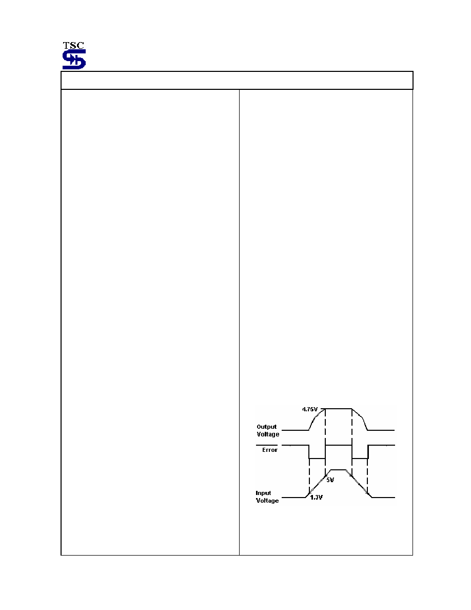
Error Detection Comparator Output
The Compactor produces a logic low output whenever
the TS2951/A output falls of regulation by more than
around 5%. This is around 60 mV offset divided by the
1.235 reference voltage. Thus trip remains 5% below
nominal regardless of the programmed output voltage
of the regulator. The Figure 1 shows the timing diagram
depicting the ERROR signal and the regulator output
voltage as the TS2951/A input is ramped up and down.
The ERROR signal becomes low at around 1.3V input,it
goes high around 5V input (input voltage at which
Vout=4.75V). The TS2951/A dropout voltage depending
on the load, the input voltage trip point around 5V will
vary with load current. The output voltage trip point is
around 4.75V, it does not change with load. The error
comparator has an open-collector output which requires
an external pull-up resistor. Depending on the system
requirement, the resistor maybe returned to 5 or 3.3V
output or other supply voltage depending to the system
requirements. For determining the size of the resistor,
note that the output is sinking 400uA, this value adds to
battery drain in a low better condition, recommended
values 100K to 1M. If the output is unused this
resistor is not required.
Figure 1. Error Output Timing
TS2950-51 series
5-6
2003/12 rev. B
Application Hints (continued)
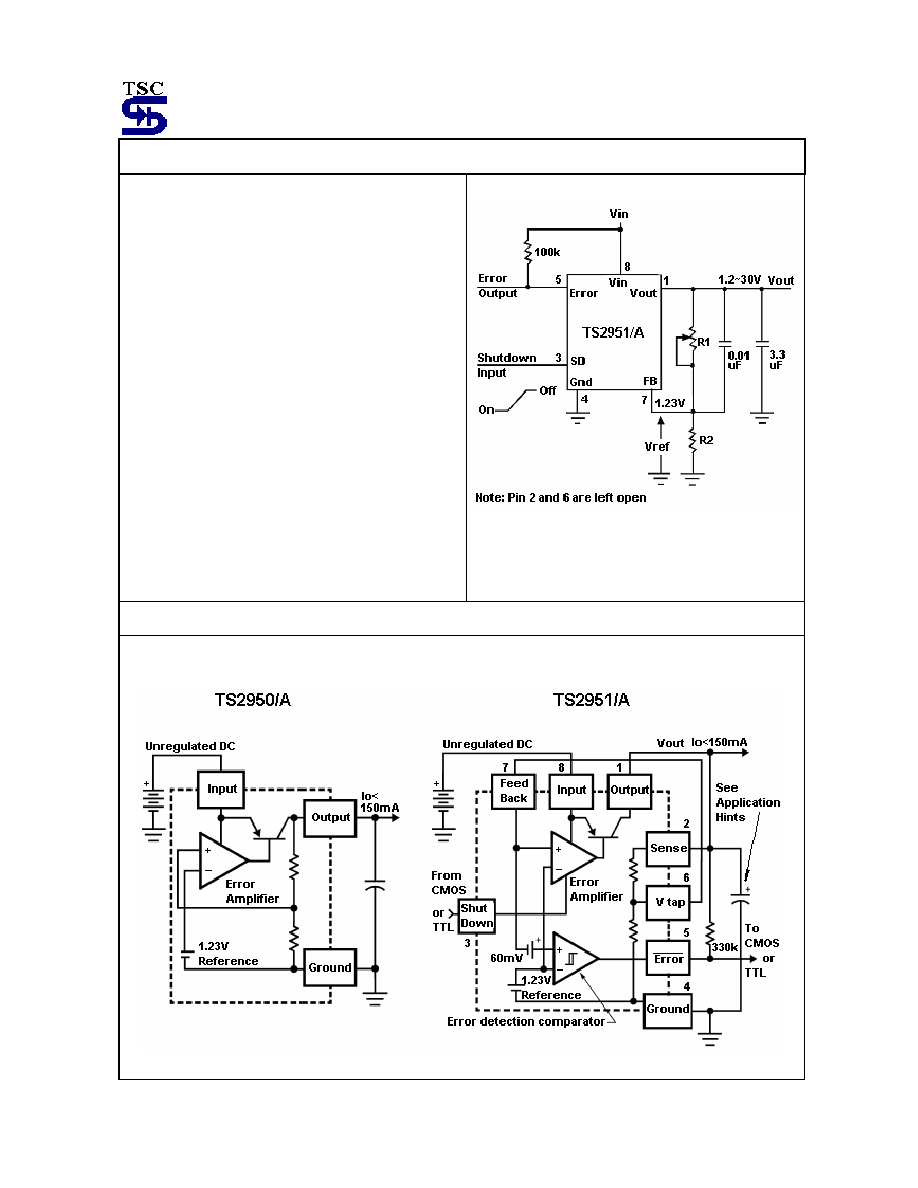
Programming The output Voltage
The TS2951/A output voltage is programmable for any
value from it reference voltage of 1.235V and it maximum
rating of 30V. For example for 5 volt needs to
pin-strapped and using the internal voltage divider by
tying pin 1 to 2 and pin 7 to pin 6. Refer to Figure 2, there
are two external resistor required for this programming.
Refer to the below equation for the programming the
output voltage:
Volt=Vref x (1+R1\R2)+I
FB
* R1
The Vref is 1.235V and I
FB
is the feedback bias current,
nominally -20nA. The minimum recommended load
current of 1uA forces an upper limit of 1.2Mon value of
R2, If no load presented the I
FB
produces error of typically
2% in Vout which maybe eliminated at room temperature
by trimming R1. To improve the accuracy chooses the
value of R2=100K and this reduces the error by 0.17%
and increases the resistor program current by 12uA. The
TS2951/A typically draw 60uA at no load with pin 2
open-circuit, and this value does not look much.
Figure 2. Adjust Voltage
Block Diagram and Typical Applications Circuit