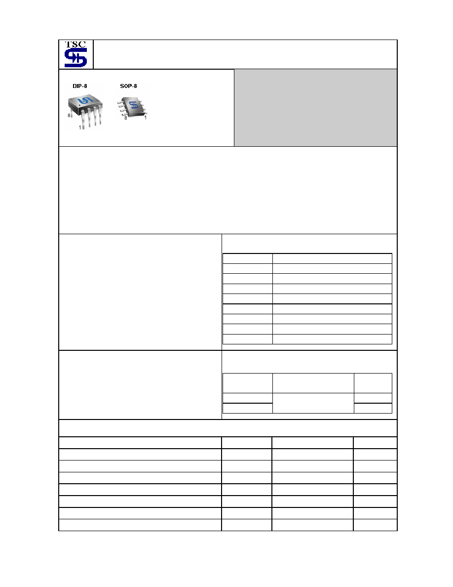
TS3404 1-5
2003/12
rev.
A
TS3404
PWM Buck Controller
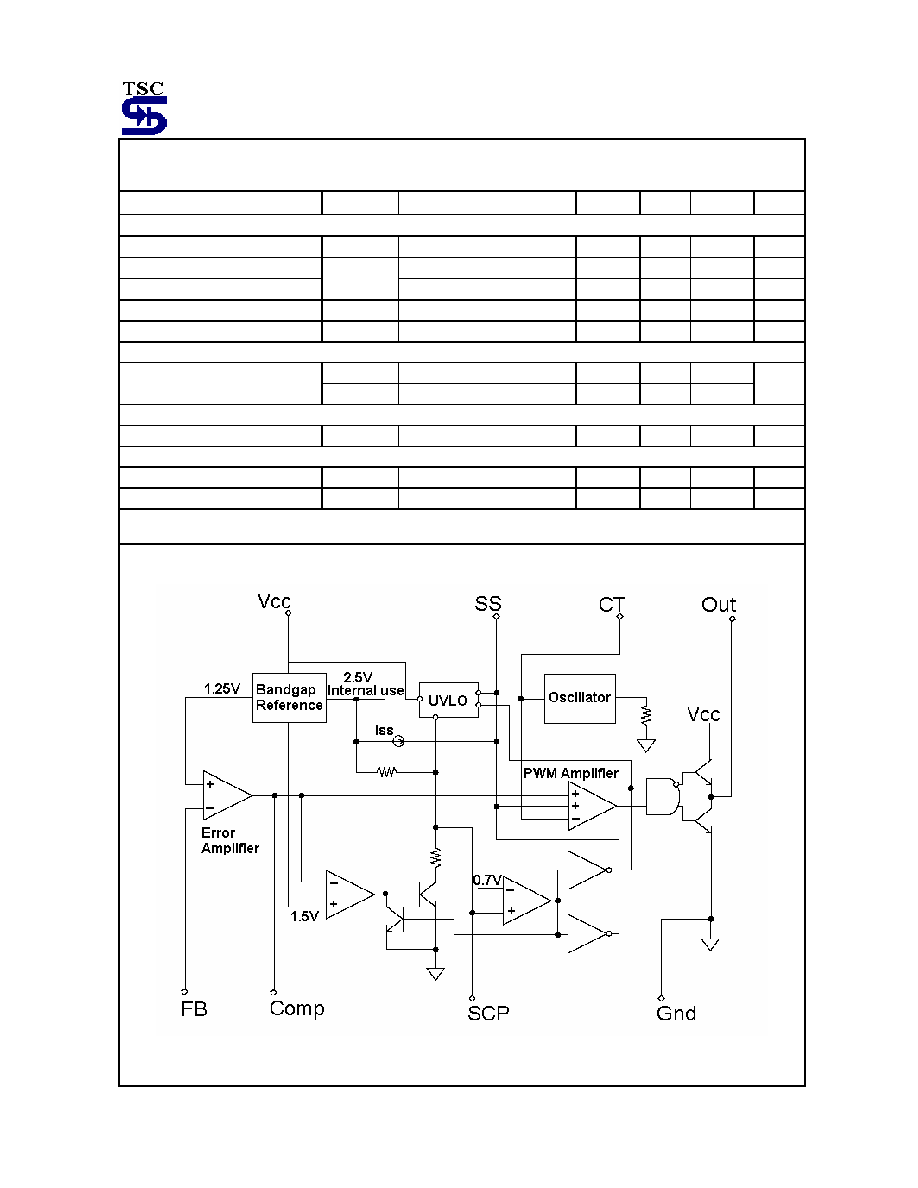
Pin assignment:
1. Out
2. Vcc
3. Comp.
4. FB
5. SCP
6. SS
7. CT
8.
Gnd
Supply Voltage Range 3.6V to 27V
Output Driving Current 200mA
Oscillator Frequency up to 300KHz
General Description
The TS3404 integrates Pulse Width Modulation (PWM) control circuit into a single chip, and makes simple work out of
implementing a complete control and protection scheme for a DC-DC step-down converter. The TS3404 provides simple
feedback loop compensation, 1.25V reference output, error amplifier, adjustable oscillator, soft start, under voltage lock
out (UVLO), short circuit protection(SCP) circuitry, and push pull output circuit.
The TS3404 is design for adjustable switching frequency by trimming time capacitor (CT), during low supply voltage
situation, the under voltage lock out (UVLO) makes sure that the output are off until the internal circuit operates normally.
The TS3404 is offered in DIP-8 and SOP-8 package.
Features
PWM buck control circuit
Operating voltage can be up to 27V
Under voltage lock out (UVLO) protection
Soft start (SS) circuit
Short circuit Protection (SCP)
Variable oscillator frequency 300KHz (max)
1.25V voltage reference Output
Pin Descriptions
Name Description
Output PWM
Output
Vcc Supply
Voltage
Comp.
Feedback Loop Compensation
FB Voltage
Feedback
SCP Short
Circuit
Protection
SS Soft
Start
CT Timing
Capacitor
Gnd Ground
Applications
LCD
Monitor
xD-ROM, xDSL product
DC to DC converters in computers
Backlight inverter
Ordering Information
Part No.
Operating Temp.
(Ambient)
Package
TS3404CS SOP-8
TS3404CD
-20 ~ +85
o
C
DIP-8
Absolute Maximum Rating
Supply Voltage
V
CC
28
V
Amplifier Input Voltage
V
I
20
V
Collector Output Voltage
V
O
Vcc~1.0V V
Source Current
I
SOURCE
200 mA
Sink Current
I
SINK
200 mA
Operating Junction Temperature Range
T
J
-20
~
+150
o
C
Storage Temperature Range
T
STG
-65
~
+150
o
C
Lead Temperature 1.6mm(1/16") from case for 10Sec.
T
LEAD
260
o
C
TS3404 2-5
2003/12
rev.
A
Recommended Operating Conditions
Parameter Symbol.
Min.
Max.
Unit
Supply voltage
V
CC
3.6
27
V
Amplifier input voltage
V
I
1.05
1.45
V
Collector output voltage
V
O
Vcc~1.5
V
Current into feedback terminal
I
FB
45
uA
Feedback resistor
R
F
100 K
Timing capacitor
C
T
100
6800
pF
Oscillator frequency
F
OSC
10 300
KHz
Electrical Characteristics
(V
CC
=6V, f = 200KHz, Ta =25
o
C; unless otherwise specified.)
Parameter Symbol
Test
Conditions Min
Typ
Max
Unit
Reference
Comp. Connect to FB
1.225
1.25
1.275
V
Ta= -20
o
C ~ 25
o
C
-
0.1
1
Output voltage change with
temperature
V
REF
Ta= 25
o
C ~ 85
o
C
-
0.2
1
%
Under voltage lock out (UVLO)
Upper threshold Voltage
V
UT
2.9
Lower threshold voltage
V
LWT
2.4
Hysteresis V
HT
I
O(REF)
= 0.1mA, Ta= 25
o
C
0.5
V
Short circuit protection (SCP)
Input threshold voltage
V
iT
Ta=
25
o
C
0.60 0.67 0.75 V
Standby voltage
V
STB
No pull up
100
130
160
mV
Latched input voltage
V
LT
No pull up
50
100
mV
Input (source) current
I
SCP
V
I
= 0.7V, Ta= 25
o
C
- 10
- 15
- 20
uA
Comparator threshold voltage
V
CT
1.5 V
Oscillator (OSC)
Frequency F
OSC
C
T
= 270pF
200
KHz
Standard deviation of frequency
C
T
=
270pF
10
Frequency change with voltage
F
OSC
V
CC
= 3.6V ~ 20V
1
%
Error Amplifier
Input offset voltage
V
IO
�
6
mV
Input offset current
I
IO
�
100
nA
Input bias current
I
IB
V
O
(FB)= 1.25V
160
500
nA
Common mode input voltage
range
V
CM
V
CC
= 3.6V ~ 20V
1.05
1.45
V
Open loop voltage amplification
AV
R
F
= 200k
70
80
dB
Unity gain bandwidth
GBW
1.5
MHz
Common mode reject ratio
CMRR
60
80
dB
Max. output voltage
V
OH
V
REF
~0.1
V
Min. output voltage
V
OL
1 V
Output (sink) current (Comp)
I
OI
0.5
1.6
mA
Output (source) current (Comp)
I
OO
V
ID
= - 0.1V, V
O
= 1.25V
- 45
- 70
uA
TS3404 3-5
2003/12
rev.
A
Electrical Characteristics
(Continued)
(V
CC
=6V, f = 200KHz, Ta =25
o
C; unless otherwise specified.)
Parameter Symbol
Test
Conditions Min
Typ
Max
Unit
Output section
Leakage current
I
LEAK
V
O
= 25V
10
uA
Sink current
V
IN
= 20V
200
mA
Source current
I
DRV
V
IN
= 20V
200
mA
Output saturation voltage
V
SAT
I
O
= 10mA
1.0
1.5
V
Short circuit output current
I
SC
V
O
= 6V
120
mA
PWM comparator
V
TO
CT
0.6 0.7
Input threshold voltage at
f =10KHz (Comp)
V
T100
Maximum duty cycle
1.2
1.3
V
Total device
Average supply current
I
CCA
C
T
= 270pF
6
10
mA
Soft Start
Soft start voltage
V
SS
2.3 V
Constant charge current
I
SS
20 uA
Functional Block Diagram
TS3404 4-5
2003/12
rev.
A
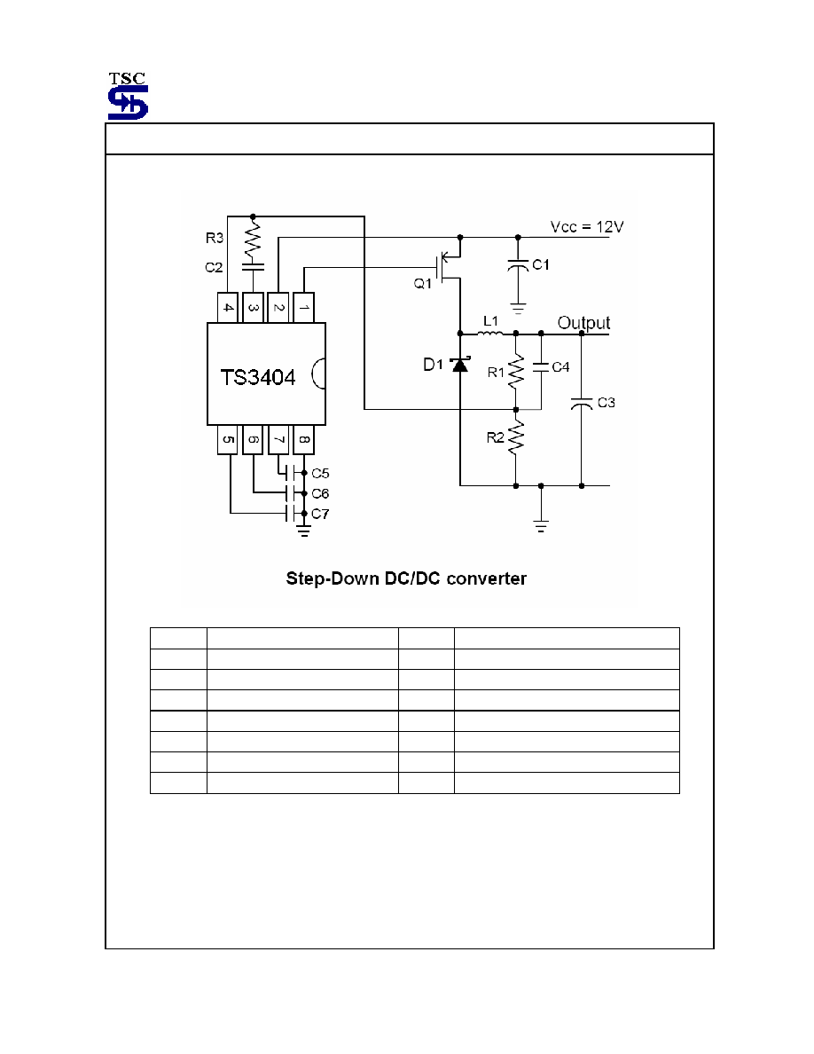
Typical Application Circuit
Device Value Device
Value
C1 470uF R1 9K,
1/4W
C2 10nF R2 3K,
1/4W
C3 470uF R3 10K,
1/4W
C4 50nF L1 33uH,
3A
C5 270uF D1
SK34A
C6 50nF Q1 TSM2301CX
C7 220nF
Remark:
* Output = 1.25V * (R1/R2 +1) = 1.25V * (9K/3K + 1) = 5V @ 3A
* SK34A: Taiwan semiconductor, Schottky 3A/40V in SMA package
* TSM2301CX: Taiwan semiconductor, P-Channel MOSFET 4A/20V in SOT-23 package
TS3404 5-5
2003/12
rev.
A
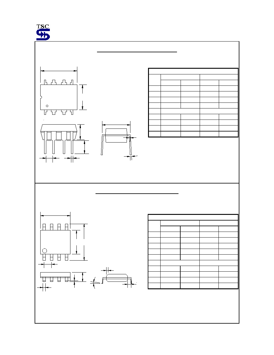
DIP-8 Mechanical Drawing
C
K
D
G
B
A
1
8
4
5
L
M
J
DIP-8 DIMENSION
MILLIMETERS INCHES
DIM
MIN MAX MIN MAX
A 9.07 0.32 0.357 0.367
B 6.22 6.48 0.245 0.255
C 3.18 4.43 0.125 0.135
D 0.35 0.49 0.019 0.020
G
2.54 (typ)
0.100 (typ)
J 0.29 0.31 0.011 0.012
K 3.25 3.35 0.128 0.132
L 7.75 8.00 0.305 0.315
M - 10
o
- 10
o
SOP-8 Mechanical Drawing
C
P
B
D
K
G
1
8
A
16
9
R
M
F
SOP-8 DIMENSION
MILLIMETERS INCHES
DIM
MIN MAX MIN MAX
A 4.80 5.00 0.189 0.196
B 3.80 4.00 0.150 0.157
C 1.35 1.75 0.054 0.068
D 0.35 0.49 0.014 0.019
F 0.40 1.25 0.016 0.049
G
1.27 (typ)
0.05 (typ)
K 0.10 0.25 0.004 0.009
M 0
o
7
o
0
o
7
o
P 5.80 6.20 0.229 0.244
R 0.25 0.50 0.010 0.019