TS34063A
1-8
2005/02 rev. A
TS34063AA
Dc to Dc Converter Controller
Supply Voltage Range 3 V to 40V
Output Driving Current 1.5A
Oscillator Frequency up to 100KHz
General Description
The TS34063A is a monolithic switching regulator and subsystem intended for use as DC to DC converter. It contains an
internal temperature compensated reference, comparator, controlled duty cycle oscillator with an active peak current limit
circuit, drive and a high current output switch.
The TS34063A is specifically designed to be incorporated in step-up, step-down and voltage inverting converter
applications.
The TS34063A is offered in SOP-8 and DIP-8 package.
Features
Power forward control circuit
Operating voltage form 3V to 40V
Low standby current
Current limit adjustable
Output switch current up to 1.5A
Variable oscillator frequency up to 100KHz (max)
Output voltage adjustable
Pin Descriptions
Name Description
SC Switch
Collector
SE Switch
Emitter
CT Timing
Capacitor
Gnd Ground
Comp.
Comparator Inverting Input
Vcc Vcc
Collector
Ipk Ipk
Sense
Vdriver Driver
Applications
Charger
xD-ROM, xDSL product
DC to DC converter s
Ordering Information
Part No.
Operating Temp.
(Ambient)
Package
TS34063ACD
DIP-8
TS34063ACS
-20 ~ +85
o
C
SOP-8
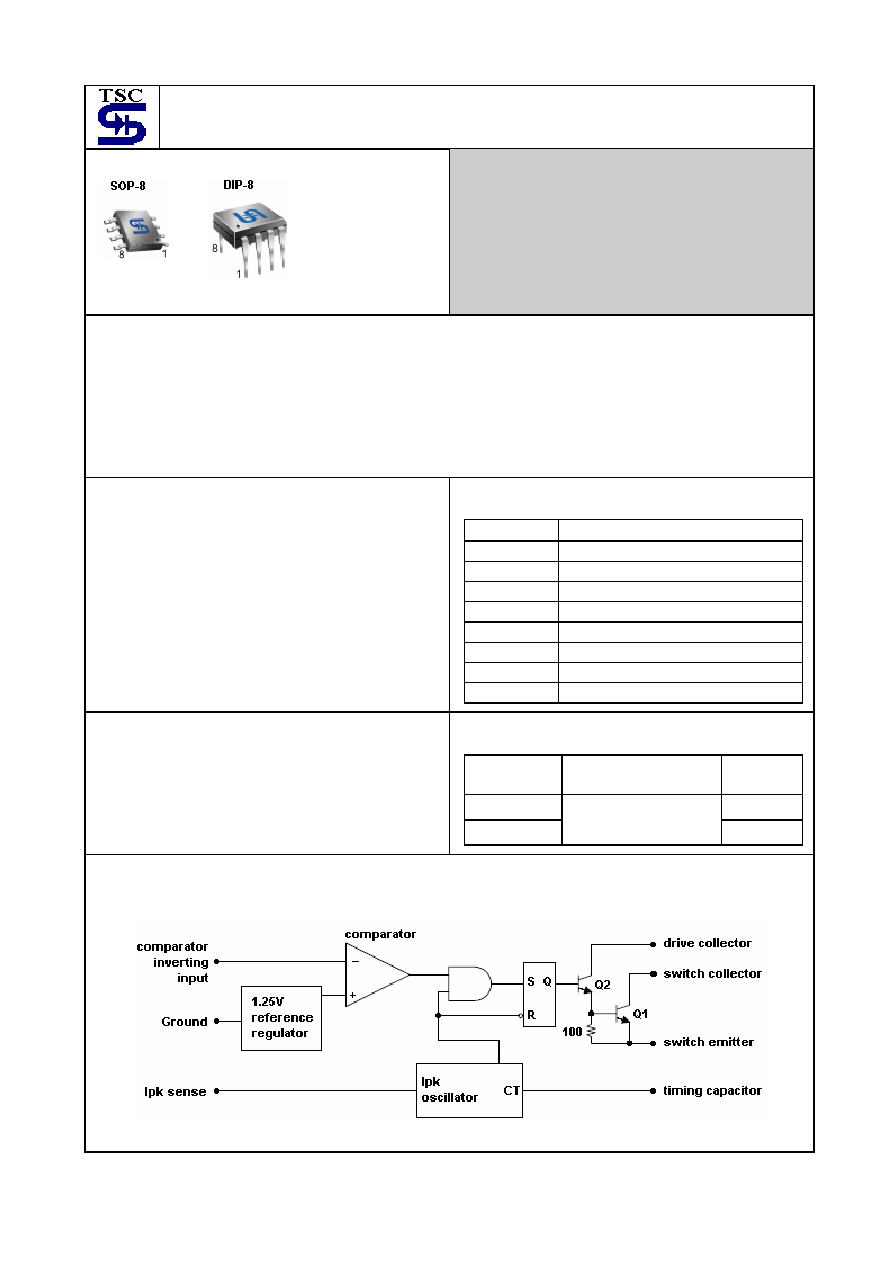
Block Diagram
Pin assignment:
1. SC
2. SE
3. CT
4. Gnd
5. Comp.
6. Vcc
7. Ipk
8. Vdriver
TS34063A
2-8
2005/02 rev. A
Absolute Maximum Rating
Supply Voltage
V
CC
40 V
Comparator Input Voltage Range
V
FB
- 0.3 ~ 40
V
Switch Collector Output Voltage
V
C(SW)
40 V
Switch Emitter Voltage
V
E(SW)
40 V
Switch Collector to Emitter Voltage
V
CE(SW)
40 V
Driver Collector Voltage
Vc(driver)
40
V
Driver Collector Current (note 1)
Ic(driver)
100
mA
Output Switching Current
I
SW
1.5 A
Power Dissipation DIP-8
SOP-8
Pd
1.0
0.5
W
Operating Junction Temperature Range
T
J
-0 ~ +125
o
C
Storage Temperature Range
T
STG
-65 ~ +150
o
C
Note: Maximum package power dissipation limits must be observed
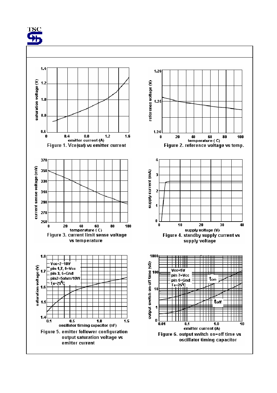
Electrical Characteristics
(V
CC
=5V, Ta =25
o
C; unless otherwise specified.)
Parameter Symbol
Test
Conditions
Min
Typ
Max
Unit
Oscillator (OSC)
Frequency F
OSC
C
T
= 1nF, Vpin5= 0V
24
33
42
KHz
Charge Current
I
CHARGE
V
CC
= 5V ~ 40V
--
30
--
uA
Discharge Current
I
DISCHARGE
V
CC
= 5V ~ 40V
--
200
--
uA
Discharge to Charge current ratio
I
DISCHARGE
/ I
CHARGE
Pin7 to Vcc
--
6.5
--
--
Current Limit Sense Voltage
V
IPK(SENSE)
I
DISCHARGE
= I
CHARGE
250
--
350
mV
Output switch (note1)
Saturation Voltage
V
CE(SAT)
I
SW
= 1A, pin1,8 connected)
--
1.0
1.3
V
Saturation Voltage
V
CE(SAT)
I
SW
= 1A, Id=50mA
--
0.45
0.7
V
DC current gain
H
FE
I
SW
= 1A, Vce= 0.5V
--
75
--
--
Collector off-state current
I
C(OFF)
Vce= 40V
--
0.01
100
uA
Comparator
Threshold Voltae
V
REF
1.225 1.25 1.275 V
Line regulation
RegLine
V
CC
= 3V ~ 40V
--
--
6
mV
Total device
Supply Current
I
CC
V
CC
= 5V ~ 40V, C
T
= 1nF,
pin7=Vcc, pin5>Vth,
pin2=Gnd, remaining pins
open
-- 1.6 3 mA
Note: 1. Low duty cycle pulse techniques are used during test to maintain junction temperature as close to ambient
temperature as possible
2. If the output switch is driven into hard saturation (non-Darlington configuration) at low switch currents (<=300mA)
and high driver currents (>=30mA), it may take up to 2uS for it to come out of saturation. This condition will
shorten the off time at frequencies >= 30KHz, and is magnified at high temperature. This condition does not
occur with a Darlington configuration, since the output switch cannot saturate. If a non-Darlington configuration
is used, the following output drive condition is recommended:
Forced Bata of output switch: Ic output / (Ic driver � 7mA*) >= 10
* The 100ohm resistor in the emitter of the driver divide requires about 7mA before the output switch conducts.
TS34063A
3-8
2005/02 rev. A
Circuit Description
TS34063A
4-8
2005/02 rev. A
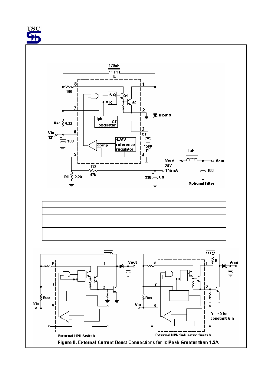
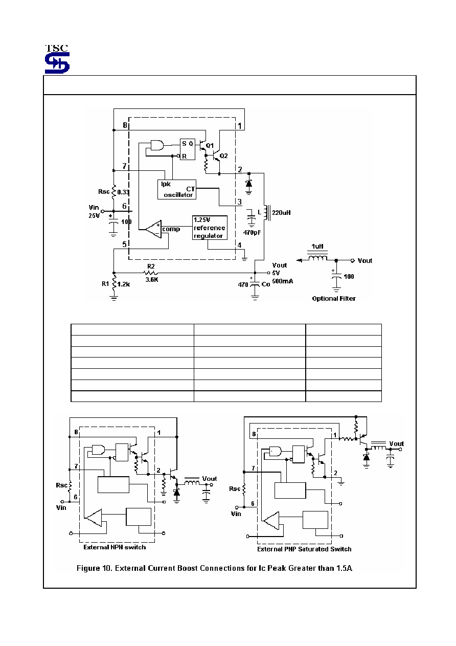
Typical Application Circuit
Figure 7. Step Up Converter
Test Conditions
Results
LINE REGULATION
Vin= 8V~16V, Io= 175mA
30mV +/- 0.05%
Load Regulation
Vin= 12V, Io= 75mA to 175mA
10mV +/- 0.017%
Output Ripple
Vin=12V, Io= 175mA
400mVpp
Efficiency
Vin=12V, Io= 175mA
87.7%
Output Ripple with Optional Filter
Vin=12V, Io= 175mA
40mVpp
TS34063A
5-8
2005/02 rev. A
Typical Application Circuit (continues)
Figure 9. Step Down Converter
Test Conditions
Results
Line Regulation
Vin= 15V~25V, Io= 500mA
12mV +/- 0.12%
Load Regulation
Vin= 25V, Io= 50mA to 500mA
3mV +/- 0.03%
Output Ripple
Vin= 25V, Io= 500mA
120mVpp
Short Circuit Current
Vin= 25V, RL= 0.1ohm
1.1A
Efficiency
Vin= 25V, Io= 500mA
83.7%
Output Ripple with Optional Filter
Vin= 25V, Io= 500mA
40mVpp
TS34063A
6-8
2005/02 rev. A
Typical Application Circuit (continues)
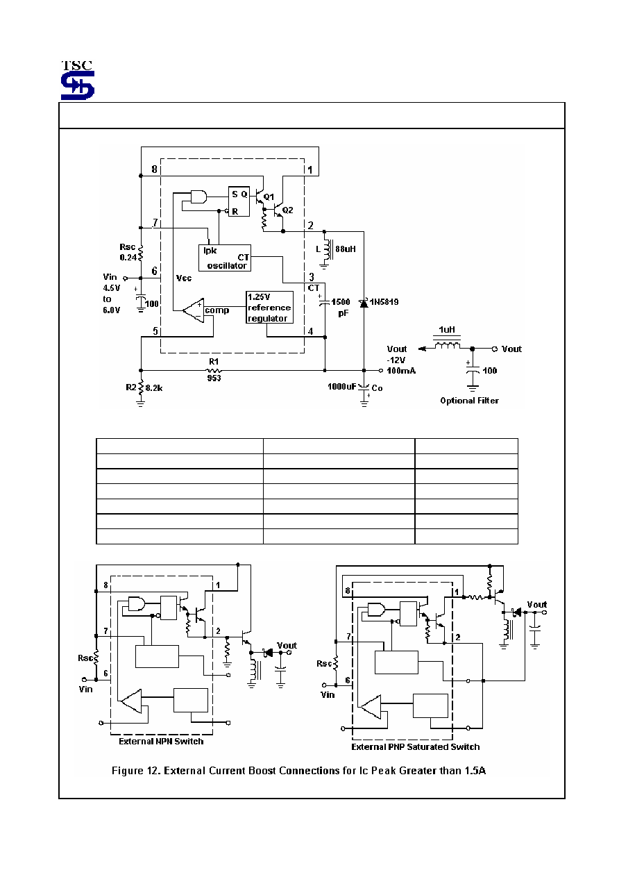
Figure 11. Voltage Inverting Converter
Test Conditions
Results
Line Regulation
Vin= 4.5V~6.0V, Io= 100mA
3mV +/- 0.012%
Load Regulation
Vin= 5V, Io= 10mA to 100mA
22mV +/- 0.09%
Output Ripple
Vin= 5V, Io= 100mA
500mVpp
Short Circuit Current
Vin= 5V, RL= 0.1ohm
900mA
Efficiency
Vin= 5V, Io= 100mA
62.2%
Output Ripple with Optional Filter
Vin= 5V, Io= 100mA
70mVpp
TS34063A
7-8
2005/02 rev. A
Design Formula Table
Test
Step Up
Step Down
Voltage Inverting
t
on
t
off
Vsat
Vcc
Vin
Vf
Vout
-
-
+
(min)
(min)
Vout
Vsat
Vcc
Vf
Vout
-
-
+
Vsat
Vcc
Vf
Vout
-
+
|
|
(
t
on+
t
off )
min
1
f
min
1
f
min
1
f
CT
4.0 x 10
�5
t
on
4.0 x 10
�5
t
on
4.0 x 10
�5
t
on
Ipk(switch)
2Iout(max)
+ 1
toff
ton
2Iout(max)
2Iout(max)
+ 1
toff
ton
Rsc
)
(
3
.
0
switch
Ipk
)
(
3
.
0
switch
Ipk
)
(
3
.
0
switch
Ipk
L(min)
)
ton(
)
Ipk(switch
Vsat
)
Vin(
max
*
min
-
(max)
*
)
(
(min)
ton
switch
Ipk
Vout
Vsat
Vin
-
-
(max)
*
)
(
(min)
ton
switch
Ipk
Vsat
Vin
-
Co
)
(
*
9
pp
Vripple
ton
Iout
+
)
(
8
)
)(
(
pp
Vripple
toff
ton
switch
Ipk
)
(
*
9
pp
Vripple
ton
Iout
Terms and Definitions
Vsat = Saturation Voltage of the output switch.
Vf
= Forward Voltage drop of the rectifier.
The following power supply characteristics must be chosen:
Vin= Normal input voltage
Vout: Desied Output voltage, |Vout| =1.25 (1+R2 / R1)
Iout : Desired output current.
fmin : Minimum desired output switching frequency at the selected values for Vin
and Io.
Vripple(p-p): Desired peak-to-peak output ripple voltage. in practice, the calculated capacitor value will need to be
increased due to its equivalent series resistance and board layout. The ripple voltage should be kept to a low value
since it will directly affect the line and load regulation.
TS34063A
8-8
2005/02 rev. A
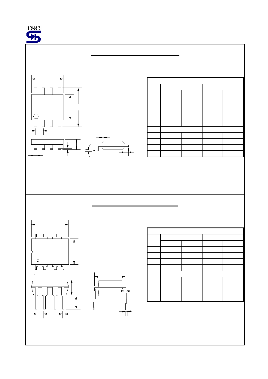
SOP-8 Mechanical Drawing
C
P
B
D
K
G
1
8
A
16
9
R
M
F
SOP-8 DIMENSION
MILLIMETERS INCHES
DIM
MIN MAX MIN MAX
A 4.80 5.00 0.189 0.196
B 3.80 4.00 0.150 0.157
C 1.35 1.75 0.054 0.068
D 0.35 0.49 0.014 0.019
F 0.40 1.25 0.016 0.049
G
1.27 (typ)
0.05 (typ)
K 0.10 0.25 0.004 0.009
M 0
o
7
o
0
o
7
o
P 5.80 6.20 0.229 0.244
R 0.25 0.50 0.010 0.019
DIP-8 Mechanical Drawing
C
K
D
G
B
A
1
8
4
5
L
M
J
DIP-8 DIMENSION
MILLIMETERS INCHES
DIM
MIN MAX MIN MAX
A 9.07 9.32 0.357 0.367
B 6.22 6.48 0.245 0.255
C 3.18 4.45 0.125 0.135
D 0.35 0.55 0.019 0.020
G
2.54 (typ)
0.10 (typ)
J 0.29 0.31 0.011 0.012
K 3.25 3.35 0.128 0.132
L 7.75 8.00 0.305 0.315
M - 10
o
- 10
o