TS39100/1/2/3
1-10
2004/06 rev. E
TS39100/1/2/3
1.0A Ultra Low Dropout Positive Voltage Regulator
Low Dropout Voltage 0.4V (typ.)
Enable Input Control
Adjustable Output
Error Flag Detection
General Description
The TS39100/1/2/3 series are 1A ultra low dropout linear voltage regulators that provide low voltage, high current output
from an extremely small package. These regulator offers extremely low dropout (typically 400mV at 1A) and very low
ground current (typically 12mA at 1A).
The TS39100/1/2/3 series are fully protected against over current faults, reversed input polarity, reversed lead insertion,
over temperature operation, positive and negative transient voltage spikes, logic level enable control and error flag which
signals whenever the output falls out of regulation.
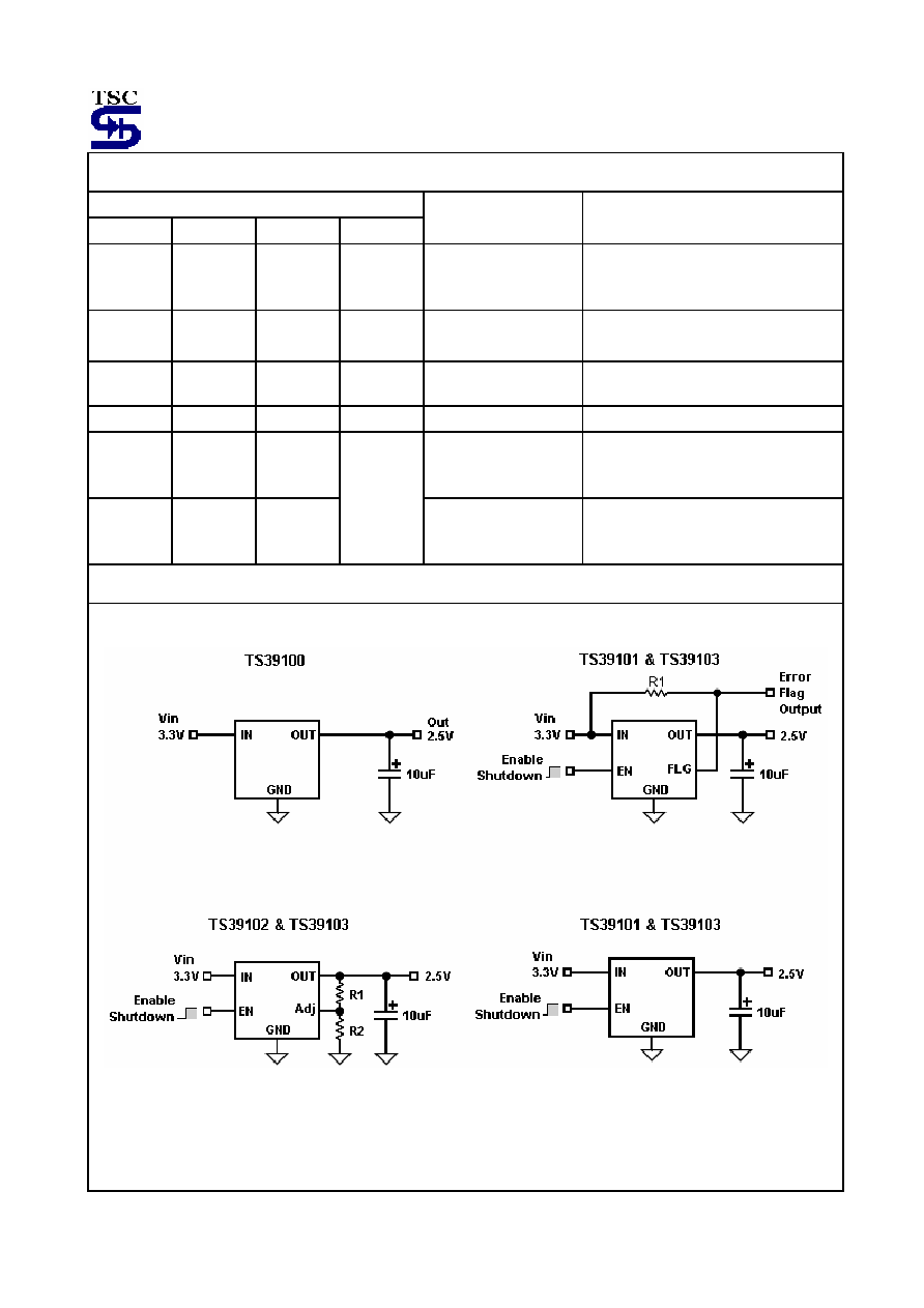
On the TS39101/2/3, the enable pin may be tied to Vin if it is not required for enable control. This series are offered in
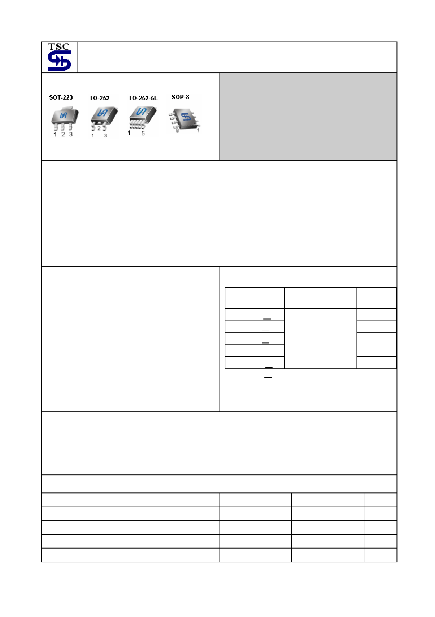
3-pin SOT-223 (TS39100), 8-pin SOP (TS39101/2) and 5-pin TO-252 (TS39103) package.
Features
Dropout voltage typically 0.4V @Io=1.0A
Output current up to 1.0A
Low ground current
Output voltage trimmed before assembly
Extremely fast transient response
Reversed leakage protection
Reverse battery protection
Error flag signals output out of regulation
Internal current limit
Thermal shutdown protection
Ordering Information
Note: Where
xx
denotes voltage option, available are
5.0V, 3.3V, 2.5V, 1.8V and 1.5V. Leave blank for
adjustable version (only TS39103). Contact to
factory for addition output voltage option.
Part No.
Operating Temp.
(Junction)
Package
TS39100CW
xx
SOT-223
TS39100CP
xx
TO-252
TS39101CS
xx
TS39102CS
SOP-8
TS39103CP5
xx
-40 ~ +125
o
C
TO-252-5L
Applications
Battery power equipment
LDO linear regulator for PC add-in cards
PowerPC
TM
power supplies
Multimedia and PC processor supplies
High efficiency linear power supplies
High efficiency post regulator for switching supply
Low-voltage microcontrollers and digital logic
SMPS post regulator
Absolute Maximum Rating
(Note 1)
Supply Voltage
Vin
-20V ~ +20
V
Enable Voltage
Ven
+20
V
Storage Temperature Range
T
STG
-65 ~ +150
o
C
Lead Soldering Temperature (260
o
C)
5
S
ESD
(Note 3)
TS39100/1/2/3
2-10
2004/06 rev. E
Operating Rating
(Note 2)
Operation Input Voltage
Vin (operate)
+2.25 ~ +16
V
Operation Enable Voltage
Ven (operate)
+2.25 ~ +16
V
Power Dissipation (Note 4)
P
D
Internally Limited
W
Operating Junction Temperature Range
T
J
-40 ~ +125
o
C
Electrical Characteristics
Vin = Vout + 1V, Venable= 2.25V, Tj = 25
o
C, unless otherwise specified.
Parameter Conditions
Min
Typ
Max
Unit
Output Voltage
I
L
=10mA 0.990|Vo|
1.010|Vo|
Output Voltage
10mA
I
L
1.0A,
Vo+1V
Vin 8V
0.980|Vo|
Vout
1.020|Vo|
V
Line Regulation
I
L
=10mA, Vo+1V
Vin 16V
--
0.05
0.5
%
Load Regulation
Vin=Vout+1V, 10mA
I
L
1A -- 0.2 1.0 %
Output Voltage Temp. Coefficient
--
40
100
ppm/
o
C
Dropout Voltage (Note 5)
Vout= -1%
I
L
=100mA
I
L
=500mA
I
L
=750mA
I
L
=1.0A
--
--
--
--
100
275
350
400
250
500
630
mV
Quiescent Current (Note 6)
Vin=V
out
+1V
I
L
=100mA
I
L
=500mA
I
L
=750mA
I
L
=1.0A
--
--
--
--
0.7
4.0
7.0
12.0
--
--
--
20
mA
Current Limited
Vout=0, Vin=Vout+1V
-- 1.8 2.5 A
Reference (TS39102)
Reference Voltage
0.980|Vo|
1.020|Vo|
Reference Voltage
(Note 7)
0.970|Vo|
1.24
1.030|Vo| V
Adjust Pin Bias Current
--
40
120
nA
Reference Voltage Temp. Coefficient
(Note 8)
--
20
--
ppm/
o
C
Adjust Pin Bias Current Temp.
Coefficient
-- 0.1 --
nA/
o
C
Flag Output (TS39101)
Output Leakage Current
V
OH
=16V --
--
2
uA
Output Low Voltage (Note 9)
Vin=0.9 * Vout, I
OL
=250uA -- -- 400 mV
Upper Threshold Voltage
% of Vout
--
--
99
%
Lower Threshold Voltage
% of Vout
93
--
--
%
Hysteresis
--
1
--
%
Enable Input (TS39101 / 2 / 3)
Low (OFF)
--
--
0.8
Input Logic Voltage
High (ON)
2.25
--
--
V
Ven=2.25V --
--
75
Enable Pin Input Current
Ven=0.8V --
--
4
uA
TS39100/1/2/3
3-10
2004/06 rev. E
Thermal Performance
Condition Package
type
Typ Unit
SOT-223 15
SOP-8 20
Thermal Resistance
Junction to Ambient
TO-252 25
o
C/W
Note 1: Absolute Maximum Rating is limits beyond which damage to the device may occur. For guaranteed
specifications and test conditions see the Electrical Characteristics.
Note 2: The device is not guaranteed to operate outside its operating rating.
Note 3: Devices are ESD sensitive. Handling precautions recommended.
Note 4: The maximum allowable power dissipation is a function of the maximum junction temperature, Tj, the junction to
ambient thermal resistance, ja, and the ambient temperature, Ta. Exceeding the maximum allowable power
dissipation will cause excessive die temperature, and the regulator will go into thermal shutdown. The effective
value of ja can be reduced by using a heatsink, Pd
(max)
= (Tj
(max)
� Ta) / ja.
Note 5: Dropout voltage is defined as the input to output differential at which the output voltage drops -1% below its
nominal value measured at 1V differential.
Note 6: Ground pin current is the regulator quiescent current. The total current drawn from the source is the sum of the
ground pin current and output load current, Iin = Ignd + Iout.
Note 7: Vref
Vout (Vin � 1V), 2.25V Vin 16V, 10mA I
L
1.0A.
Note 8: Output voltage temperature coefficient is Vout (worse cast) / (Tj
(max)
- Tj
(min)
) where is Tj
(max)
+125
o
C and
Tj
(min)
is 0
o
C.
Note 9: For adjustable device and fiexed device with Vout > 2.25V.
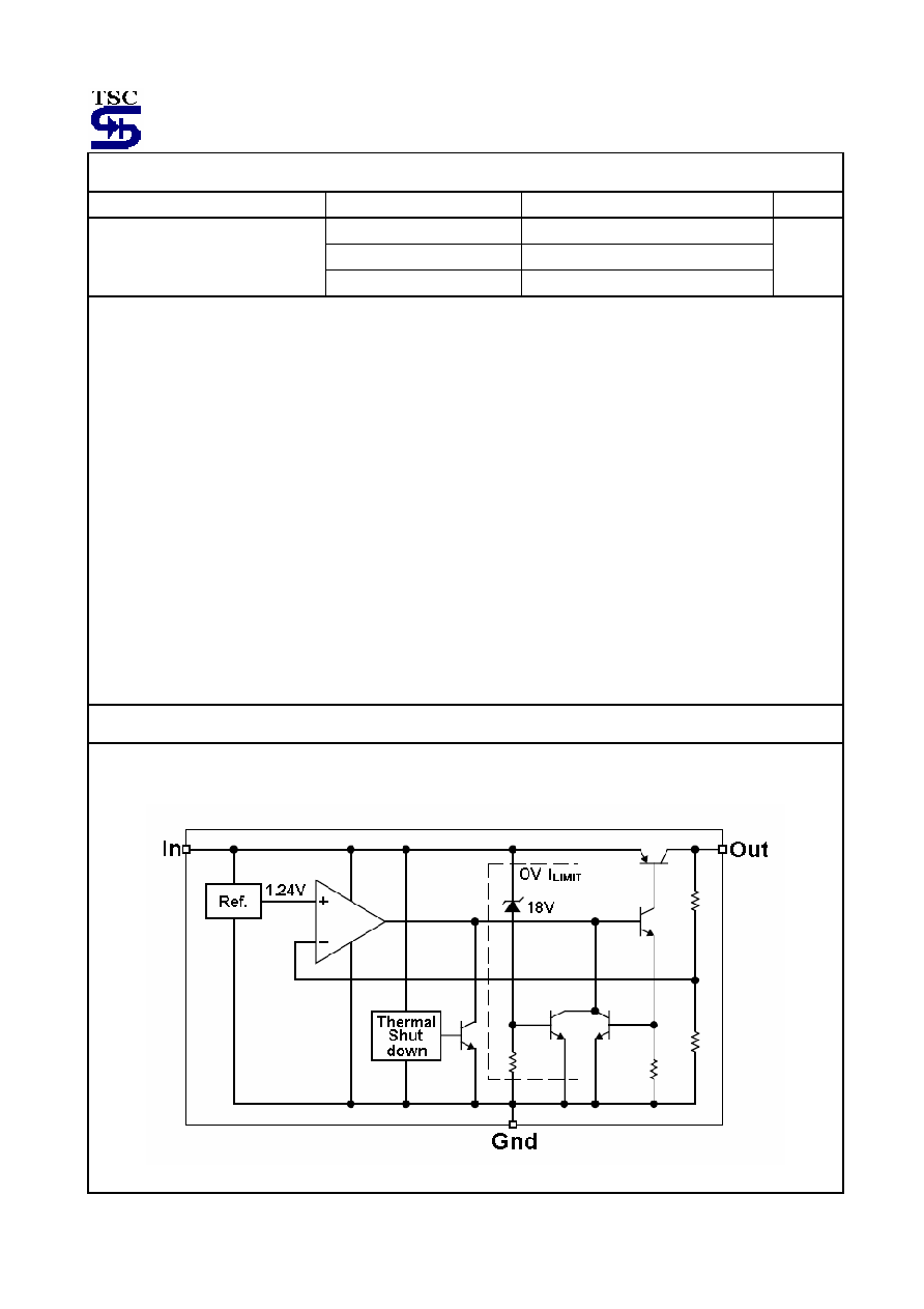
Block Diagram
TS39100
TS39100/1/2/3
4-10
2004/06 rev. E
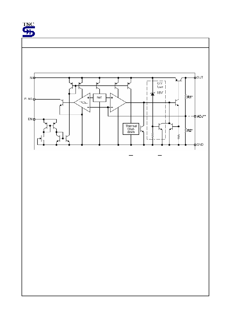
Block Diagram
TS39101 & TS39102 & TS39103
* Feedback network is fixed output versions only (TS39101CS
xx
& TS39103CP5
xx
)
** Adjustable output version only (TS39102CS & TS39103CP5)
TS39100/1/2/3
5-10
2004/06 rev. E
Pin Assignment
Pin No.
TS39100 TS39101 TS39102 TS39103
Pin Configuration
Pin
Description
1 1 1
Enable
Enable (input): TTL/COMS compatible
input. Logic high is enable; logic low or
open is shutdown
1 2 2 2
Input
Unregulated input: +26V maximum
supply
2 5,6,7,8
5,6,7,8 3
Ground
Ground: Ground pin and TAB/heatsink
are internally connected.
3 3 3 4
Output Regulator
output
4
Flag
(fixed output voltage)
Error Flag (output): Open-collector
output. Active low indicates an output
fault condition, if no used, leave open.
4
5
Feed Back
(adjustable voltage)
Adjustment input: Feedback input.
Connect to resistive voltage-divider
network.
Typical Application Circuit
TS39100/1/2/3
6-10
2004/06 rev. E
Application Information
Application Information
The TS39100/1/2/3 series are high performance with
low dropout voltage regulator suitable for moderate to
high current and voltage regulator application. Its
630mV dropout voltage at full load and over
temperature makes it especially valuable in battery
power systems and as high efficiency noise filters in
post regulator applications. Unlike normal NPN
transistor design, where the base to emitter voltage
drop and collector to emitter saturation voltage limit the
minimum dropout voltage, dropout performance of the
PNP output of these devices is limited only by low Vce
saturation voltage.
The TS39100/1/2/3 series is fully protected from
damage due to fault conditions. Linear current limiting is
provided. Output current during overload conditions is
constant. Thermal shutdown the device when the die
temperature exceeds the maximum safe operating
temperature. Transient protection allows device survival
even when the input voltage spikes above and below
nominal. The output structure of these regulators allows
voltages in excess of the desired output voltage to be
applied without reverse current flow.
Output Capacitor Requirement
The TS39100/1/2/3 series requires an output capacitor
to maintain stability and improve transient response is
necessary. The value of this capacitor is dependent
upon the output current, lower currents allow smaller
capacitors. TS39100/1/2/3 series output capacitor
selection is dependent upon the ESR of the output
capacitor to maintain stability. When the output
capacitor is 10uF or greater, the output capacitor should
have an ESR less than 2. This will improve transient
response as well as promote stability. Ultra low ESR
capacitors (<100m), such as ceramic chip capacitors,
may promote instability. These very low ESR levels may
cause an oscillation and/or under damped transient
response. A low ESR solid tantalum capacitor works
extremely well and provides good transient response
and stability over temperature aluminum electrolytes
can also be used, as long as the ESR of the capacitor is
<2.
The value of the output capacitor can be increased
without limit. Higher capacitance values help to
improve transient response and ripple rejection and
reduce output noise.
Input Capacitor Requirement
An input capacitor of 1uF or greater is recommended
when the device is more than 4" away from the bulk
AC supply capacitance or when the supply is a battery.
Small, surface mount, ceramic chip cpapcitors can be
used for bypassing. Larger values will help to improve
ripple rejection by bypassing the input to the regulator,
further improving the integrity of the output voltage.
Minimum Load Current
The TS39100/1/2/3 series is specified between finite
loads. If the output current is too small leakage
currents dominate and the output voltage rises. A
10mA minimum load current is necessary for proper
regulation.
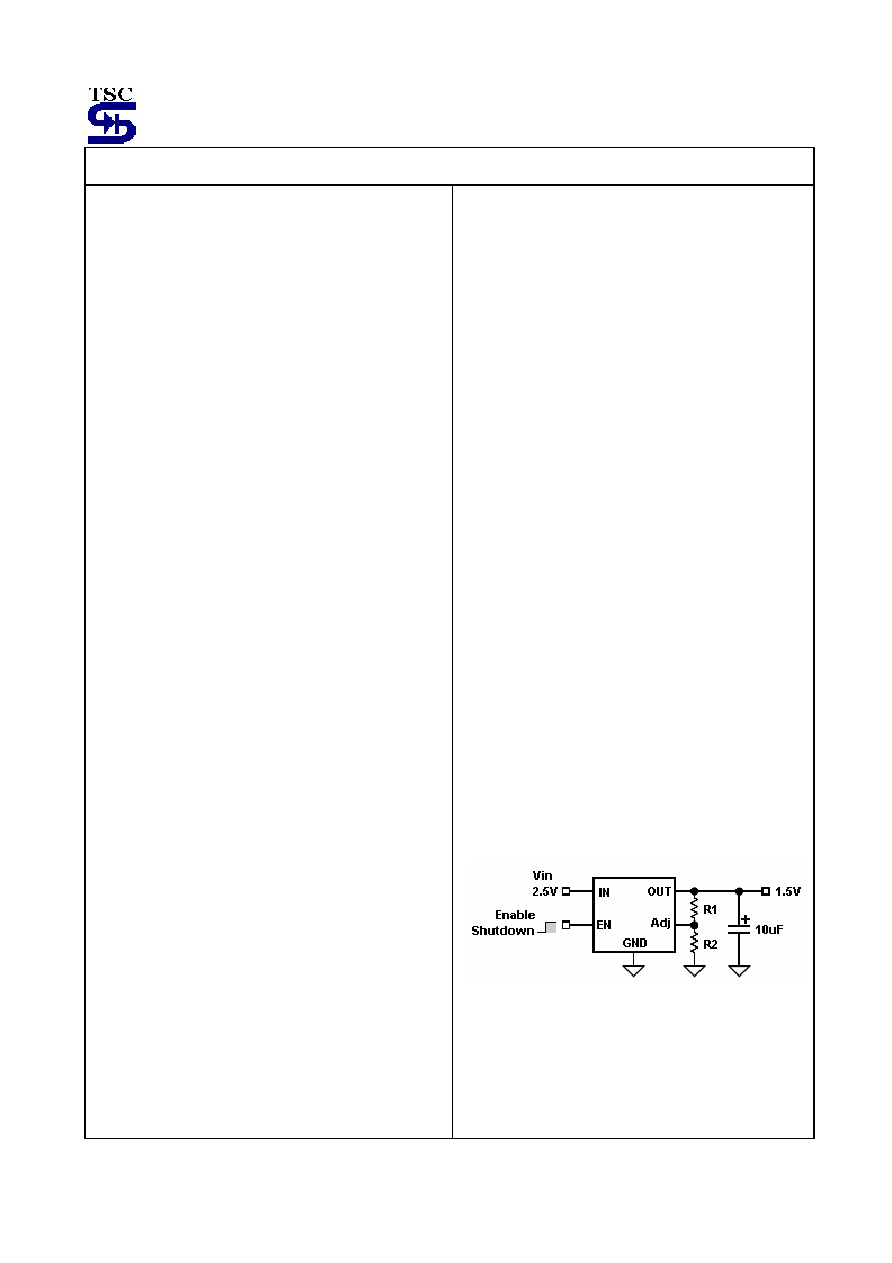
Adjustable Regulator Design
The adjustable regulator versions (TS39102) is allow
to programming the output voltage anywhere between
1.25 and the 16V maximum operating rating of the
family.
Two resistors are used. Resistors can be quite large
up to 1M, because of the very high input impedance
and low bias current of the sense comparator, the
resistor values are calculated by:
R1 = R2 * [(Vout / 1.24) � 1]
Where Vout is the desired output voltage. Above
application circuit shows component definition.
Applications with widely varying load currents may
scale the resistors to draw the minimum load current
required for proper operation.
TS39100/1/2/3
7-10
2004/06 rev. E
Application Information (continues)
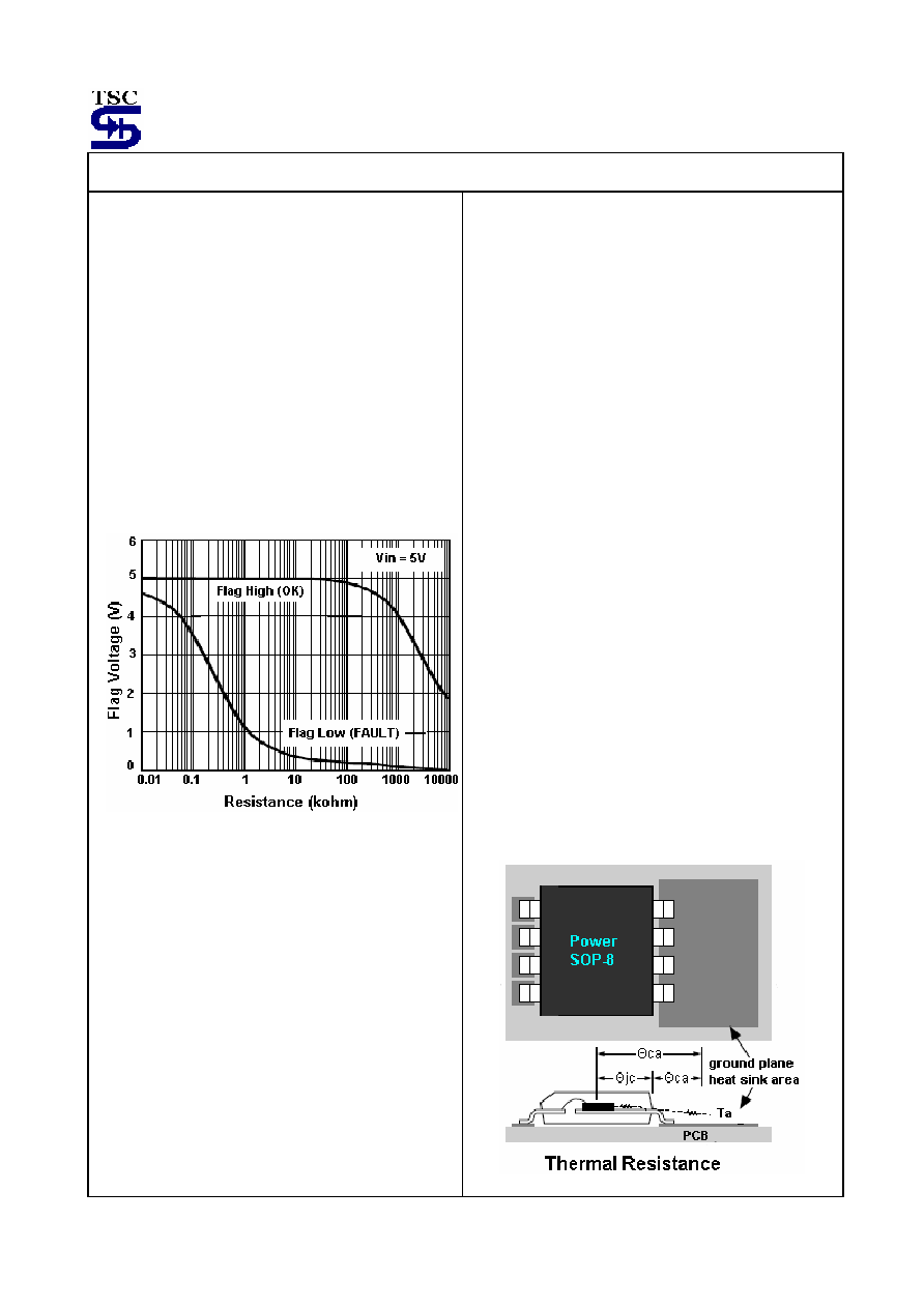
Error Flag
TS39101 versions feature an Error Flag, which looks
at the output voltage and signals an error condition
when this voltage drops 5% below its expected value.
The error flag is an open-collector output that pulls low
under fault conditions. It may sink 10mA. Low output
voltage signifies a number of possible problems,
including an over-current fault (the device is in current
limit) or low input voltage. The flag output is
inoperative during over temperature shutdown
conditions. A pull-up resistor from error flag to either
Vin or Vout is required for proper operation. For
information regarding the minimum and maximum
values of pull-up resistance, refer the graph as follow:
Enable Input
TS39101/2/3 versions feature an active-high enable
(EN) input that allows ON/OFF control of the regulator.
Current drain reduces to "zero" when the device is
shutdown, with only micro-amperes of leakage current.
The EN input has TTL/CMOS compatible thresholds
for simple interfacing with logic interfacing. EN may be
directly tied to Vin and pulled up to the maximum
supply voltage.
Transient Response and 3.3V to 2.5V
or 2.5V to 1.8V Conversion
TS39101/2/3 has excellent transient response to
variations in input voltage and load current. The device
have been designed to respond quickly to load current
variations and input voltage variations.
Large output capacitors are not required to obtain this
performance. A standard 10uF output capacitor,
preferably tantalum, is all that is required. Larger values
help to improve performance even further.
By virtue of its low dropout voltage, this device does not
saturate into dropout as readily as similar NPN base
designs. When converting from 3.3V to 2.5V or 2.5V to
1.8V, the NPN based regulators are already operating
in dropout, with typical dropout requirements of 1.2V or
greater,. To convert down to 2.5V or 1.8V without
operating in dropout, NPN based regulators require an
input voltage of 3.7V at the very least.
The TS39100 regulator will provide excellent
performance with an input as low as 3.0V or 2.5V
respectively. This gives the PNP based regulators a
distinct advantage over older, NPN based linear
regulators.
Power SOP-8 Thermal Characteristics
TS39101/2 series' performance is its power SOP-8
package featuring half the thermal resistance of a
standard SOP-8 package. Lower thermal resistance
means more output current or higher input voltage for a
given package size.
Lower thermal resistance is achieved by connect the
four ground pins with the die attached pad to create a
single piece electrical and thermal conductor. This
concept have been used by MOSFET production for
years, proving very reliable and cost effective for the
user. As under:
TS39100/1/2/3
8-10
2004/06 rev. E
Application Information (continues)
Thermal resistance consists of two main elements, jc
(junction to case) and ca (case to ambient). Using the
power SOP-8 reduces ca, the total thermal
resistance, ja (junction to ambient) is the limiting
factor in calculating the maximum power dissipation
capability of the device. Typically, the power SOP-8
have a jc of 20
o
C/W dramatically , this is significantly
lower than the standard SOP-8 which is typically
75
o
C/W. ca is reduced because pin 5~8 can be
soldered directly to a ground plane which significantly
reduces the case to sink and sink to ambient thermal
resistance.
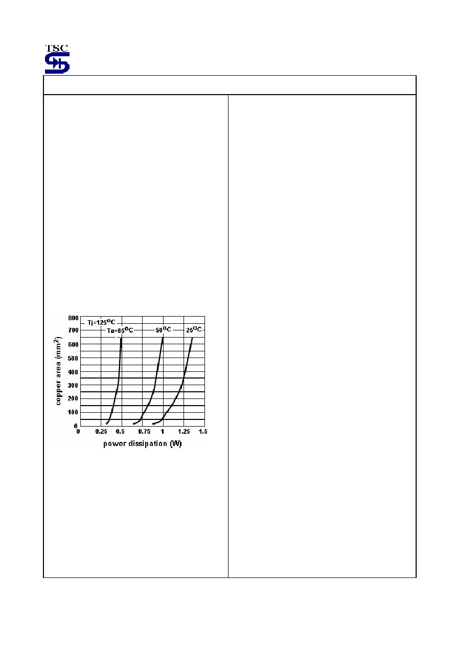
Power Dissipation
From under curves, the minimum area of copper
necessary for the par to operate safely can be
determined. The maximum allowable temperature rise
must be calculated to determine operation along
which curve.
TS39100/1/2/3
9-10
2004/06 rev. E
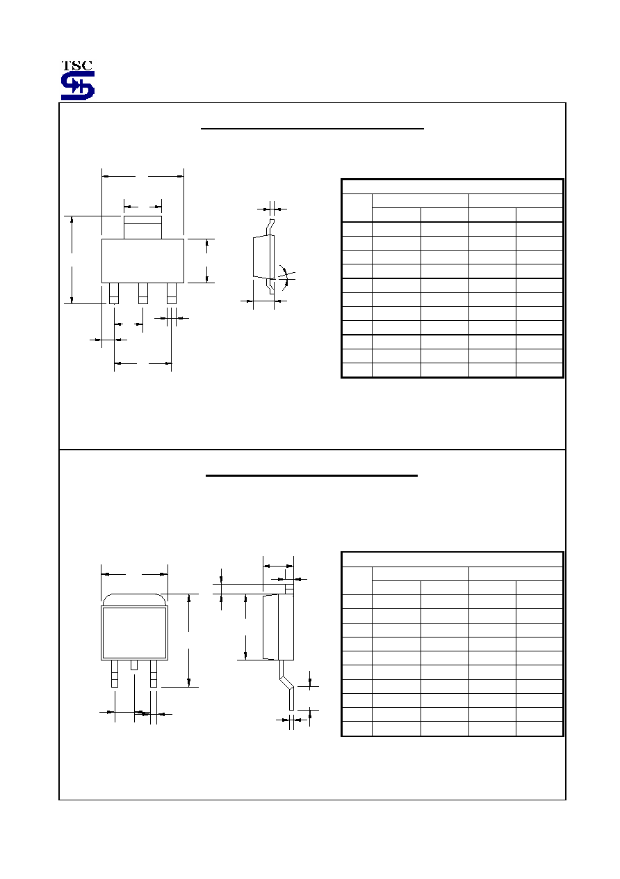
SOT-223 Mechanical Drawing
G
H
E
D
F
C
A
B
J
K
I
SOT-223 DIMENSION
MILLIMETERS INCHES
DIM
MIN MAX MIN MAX
A 6.350 6.850 0.250 0.270
B 2.900 3.100 0.114 0.122
C 3.450 3.750 0.136 0.148
D 0.595 0.635 0.023 0.025
E 4.550 4.650 0.179 0.183
F 2.250 2.350 0.088 0.093
G 0.835 1.035 0.032 0.041
H 6.700 7.300 0.263 0.287
I 0.250 0.355 0.010 0.014
J 10� 16� 10� 16�
K 1.550 1.800 0.061 0.071
TO-252 Mechanical Drawing
B
C
D
A
F
G
I
H
E
J
TO-252 DIMENSION
MILLIMETERS INCHES
DIM
MIN MAX MIN MAX
A 6.570 6.840 0.259 0.269
B 9.250 10.400 0.364 0.409
C 0.550 0.700 0.022 0.028
D 2.560 2.670 0.101 0.105
E 2.300 2.390 0.090 0.094
F 0.490 0.570 0.019 0.022
G 1.460 1.580 0.057 0.062
H 0.520 0.570 0.020 0.022
I 5.340 5.550 0.210 0.219
J 1.460 1.640 0.057 0.065
TS39100/1/2/3
10-10
2004/06 rev. E
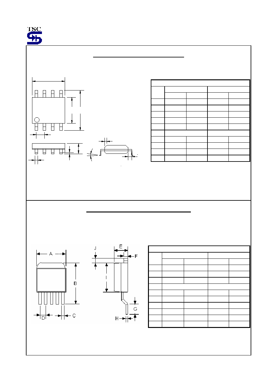
SOP-8 Mechanical Drawing
C
P
B
D
K
G
1
8
A
16
9
R
M
F
SOP-8 DIMENSION
MILLIMETERS INCHES
DIM
MIN MAX MIN MAX
A 4.80 5.00 0.189 0.196
B 3.80 4.00 0.150 0.157
C 1.35 1.75 0.054 0.068
D 0.35 0.49 0.014 0.019
F 0.40 1.25 0.016 0.049
G
1.27 (typ)
0.05 (typ)
K 0.10 0.25 0.004 0.009
M 0
o
7
o
0
o
7
o
P 5.80 6.20 0.229 0.244
R 0.25 0.50 0.010 0.019
TO-252-5L Mechanical Drawing
TO-252-5L DIMENSION
MILLIMETERS INCHES
DIM
MIN MAX MIN MAX
A 6.350 6.730 0.2509 0.265
B 9.080 10.44 0.357 0.411
C 0.460 0.640 0.018 0.025
D 1.27BSC
0.050BSC
E 2.190 2.380 0.086 0.094
F 0.460 0.570 0.018 0.022
G 1.400 1.780 0.055 0.070
H 0.460 0.570 0.018 0.022
I 5.340 5.550 0.210 0.219
J 1.520 2.030 0.060 0.080