TS4558 1-5
2003/12
rev.
A
TS4558
Dual General Purpose Operational Amplifier
Supply Voltage Range -18 V to 18V
Unity Gain Bandwidth 3MHz
Dual Channel Amplifier
General Description
The TS4558 is dual general purpose operational amplifier, and provide the high common-mode input voltage range and
the absence of latch-up make these amplifiers ideal for voltage follower application.
The devices are short circuit protected and the internal frequency compensation ensures stability without external
components.
The TS4558 is offered in 8 pin SOP-8 and DIP-8 package.
Features
Short
circuit
protection
Wide common-mode and differential ranges
No frequency compensation required
Low
power
consumption
No
latch-up
3MHz unity gain bandwidth guaranteed
Gain and phase match between amplifiers
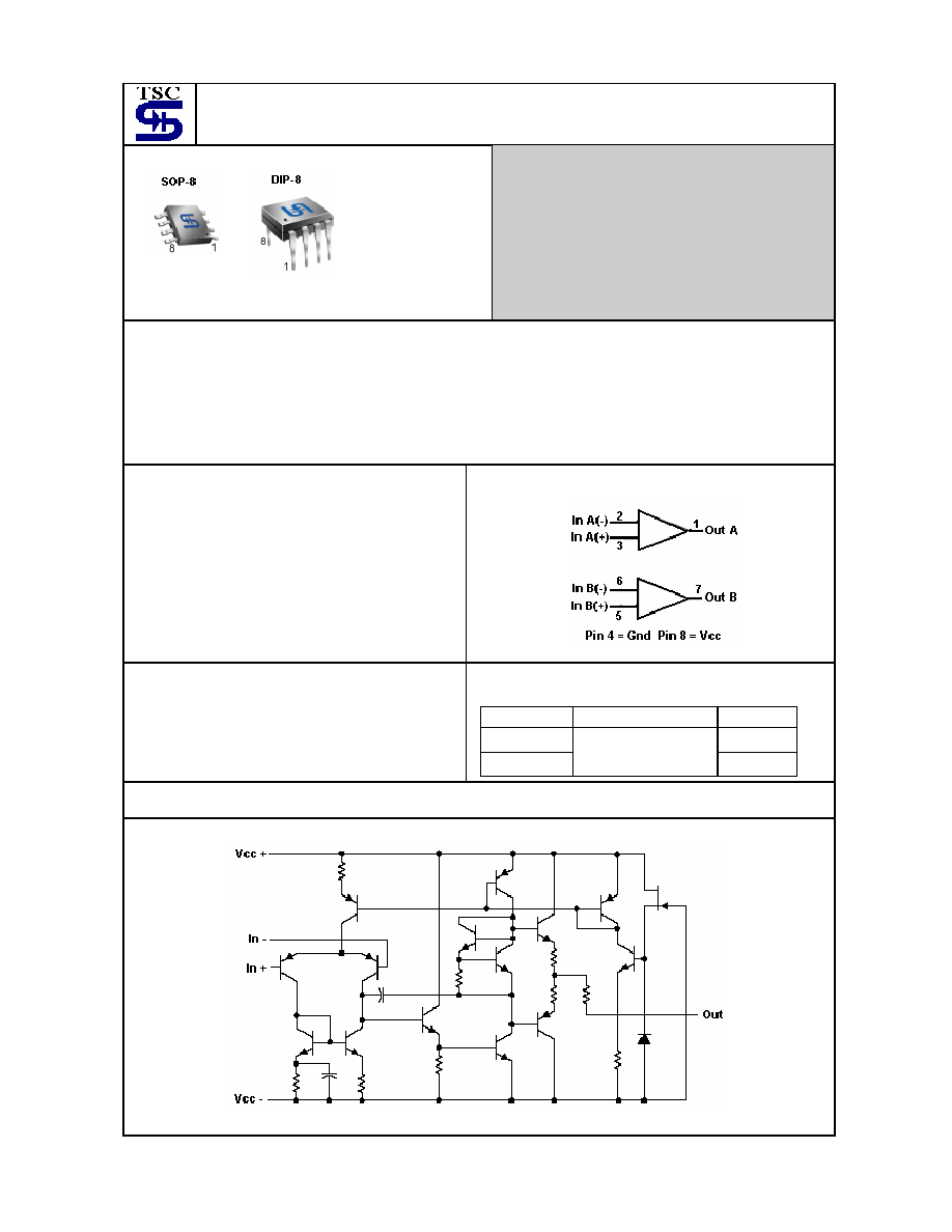
Block Diagram
Applications
DVD
player
Audio application
Ordering Information
Part No.
Operating Temp. Package
TS4558CD DIP-8
TS4558CS
0 ~ +70
o
C
SOP-8
Schematic (each amplifier)
Pin Assignment
1. Out A
2. Input A (-)
3. Input A (+)
4. Ground
5. Input B (+)
6. Input B (-)
7. Output B
8. Vcc
TS4558 2-5
2003/12
rev.
A
Absolute Maximum Rating
Supply Voltage
Vcc +
18
V
Supply Voltage
Vcc -
- 18
V
Differential Input Voltage
V
IDR
�30 V
Input Voltage
Vin
30
V
Package Thermal Impedance SOP-8
DIP-8
ja 97
85
o
C/W
Operating Junction Temperature Range
T
J
0
~
+125
o
C
Storage Temperature Range
T
STG
-65
~
+150
o
C
Lead Temperature 1.6mm(1/16") from case for 10Sec.
T
LEAD
260
o
C
Note: Maximum ratings are those values beyond which damage to the device may occur, and functional operation should
be restricted to the recommended operating condition.
Recommended Operating Conditions
Supply Voltage
Vcc +
15
V
Supply Voltage
Vcc -
- 15
V
Electrical Characteristics
(V
CC
= �15V, Ta =25
o
C; unless otherwise specified.)
Parameter Symbol
Test
Conditions
Min
Typ
Max
Unit
Input Offset Voltage
Vio
Rs 10k
0.5
�6
mV
Input Offset Current
Iio
20
�200
nA
Input Bias Current
Iib
150
500
nA
Input Resistance
Ri
0.3
5
M
Unity Gain Bandwidth
B1
3
MHz
Large-Signal Voltage Gain
Av
RL 2k, Vc = �10V
20
300
V/mV
RL 10k �12
�14
Output Voltage Swing
Vom
RL 2k �10
�14
V
Input Common-Mode Voltage
Range
Vicr
�12 �13
V
Common-Mode Rejection Ratio
CMRR
Rs 10k 70
90
dB
Supply Voltage Rejection Ratio
PSRR
Rs 10k
30
150
uV/V
Slew Rate
SR
RL = 2k, Vin=10V, L=100pF
0.8
1.6
V/uS
Supply Current
I
+
, I
-
2.5 5.6 mA
Power Consumption
Pc
RL =
75
170
mV
Input Noise Voltage
Vn
Rs = 1k, f = 30Hz~30KHz
3.5
uVrms
Source Current
Isource
- 20
mA
Sink Current
Isink
20
mA
Note 1: All characteristics are measured under open-loop conditions with zero common-mode input voltage, unless
otherwise specified.
TS4558 5-5
2003/12
rev.
A
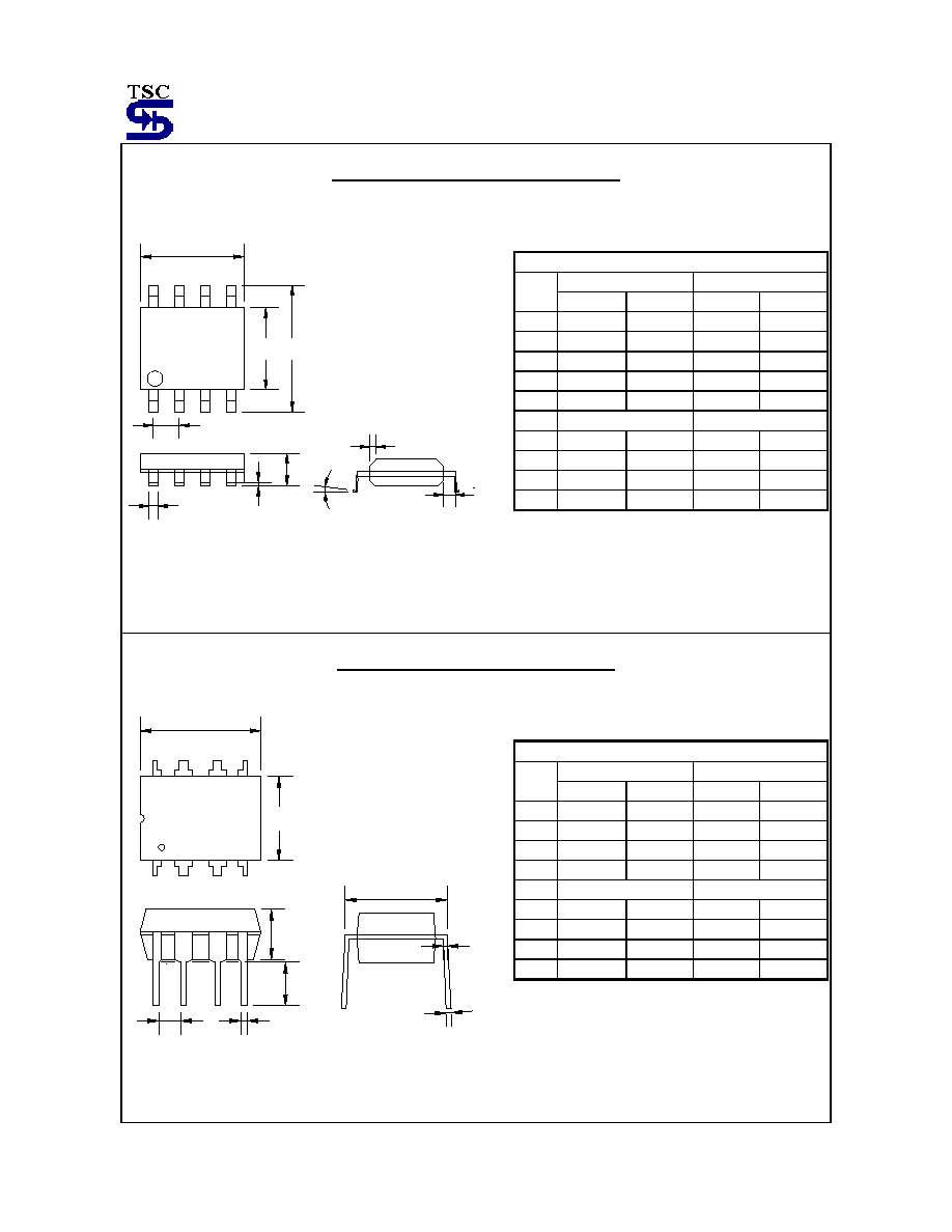
SOP-8 Mechanical Drawing
C
P
B
D
K
G
1
8
A
16
9
R
M
F
SOP-8 DIMENSION
MILLIMETERS INCHES
DIM
MIN MAX MIN MAX
A 4.80 5.00 0.189 0.196
B 3.80 4.00 0.150 0.157
C 1.35 1.75 0.054 0.068
D 0.35 0.49 0.014 0.019
F 0.40 1.25 0.016 0.049
G
1.27 (typ)
0.05 (typ)
K 0.10 0.25 0.004 0.009
M 0
o
7
o
0
o
7
o
P 5.80 6.20 0.229 0.244
R 0.25 0.50 0.010 0.019
DIP-8 Mechanical Drawing
C
K
D
G
B
A
1
8
4
5
L
M
J
SOP-8 DIMENSION
MILLIMETERS INCHES
DIM
MIN MAX MIN MAX
A 9.07 9.32 0.357 0.367
B 6.22 6.48 0.245 0.255
C 3.18 4.45 0.125 0.135
D 0.35 0.55 0.019 0.020
G
2.54 (typ)
0.10 (typ)
J 0.29 0.31 0.011 0.012
K 3.25 3.35 0.128 0.132
L 7.75 8.00 0.305 0.315
M - 10
o
- 10
o