 | –≠–ª–µ–∫—Ç—Ä–æ–Ω–Ω—ã–π –∫–æ–º–ø–æ–Ω–µ–Ω—Ç: TS494CD | –°–∫–∞—á–∞—Ç—å:  PDF PDF  ZIP ZIP |
TS494 1-7
2003/12
rev.
A
TS494
Voltage Mode PWM Controller
Supply Voltage Range 7 V to 40V
Output Driving Current 200mA
Oscillator Frequency up to 200KHz
General Description
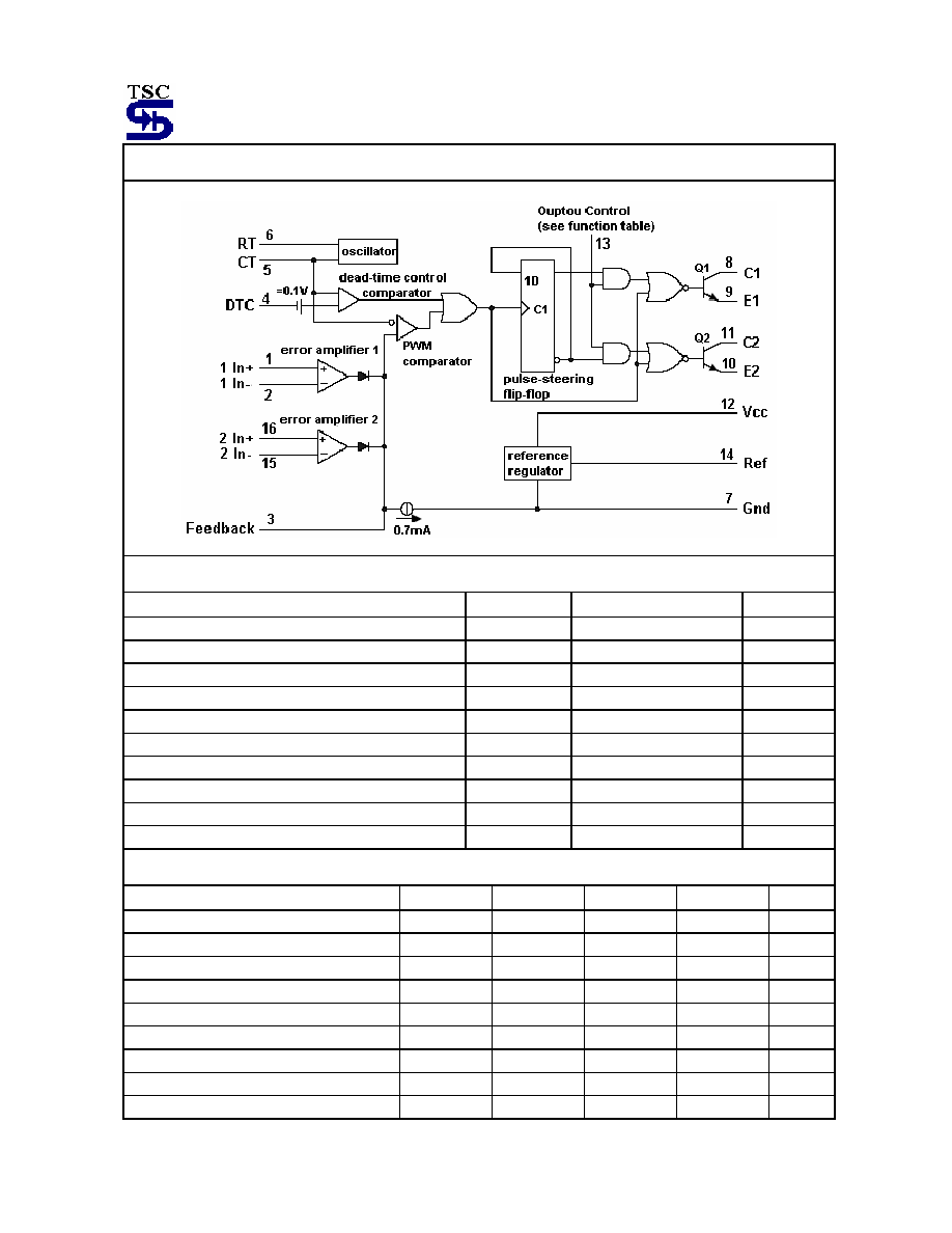
The TS494 incorporates on a single monolithic chip all the functions required in the construction of a
pulse-width-modulation control circuit. Designed primarily for power supply control, these devices offer the systems
engineer the flexibility to tailor the power supply control circuitry to his application.
The TS494 contains an error amplifier, an on-chip adjustable oscillator, a deed-time control comparator, pulse-steering
control flip-flop, a 5-volt, 5% precision regulator, and output-control circuits. The error amplifier exhibits a
common-mode voltage from ≠0.3V to Vcc ≠2V. The dead-time control comparator has a fixed offset that provides
approximately 5% dead time when externally altered. The on-chip oscillatory be bypassed by terminating R
T
(pin 6) to
the reference output and providing a sawtooth input to C
T
(pin 5), or it may be used to drive the common circuits in
synchronous multiple-rail power supplies. The uncommitted output transistor provide either common-emitter or
emitter-follower output capability. Each device provides for push-pull or single-ended output operation, which may be
selected through the output-control function. The architecture of these devices prohibits the possibility of either output
being pulsed twice during push-pull operation.
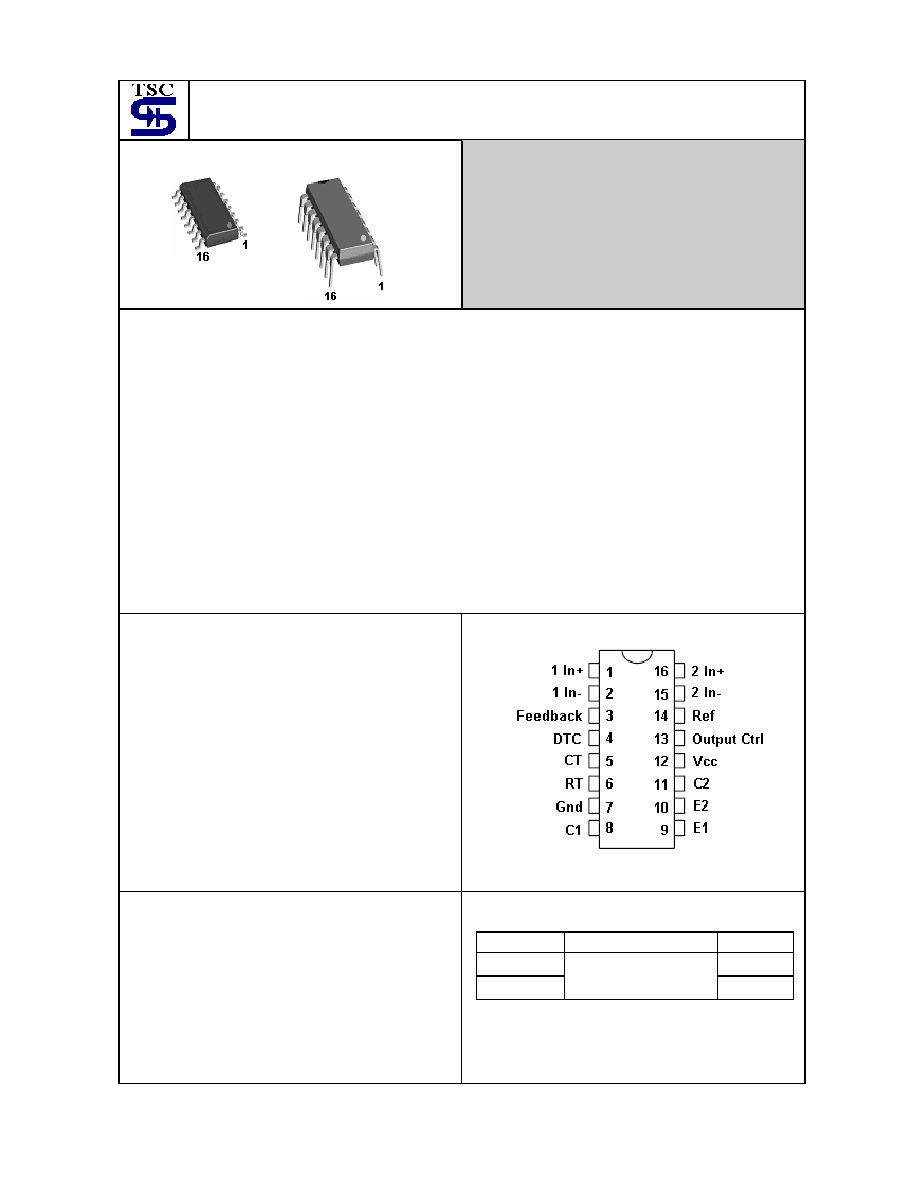
The TS494 is offered in SOP-16 and DIP-16 package.
Features
Complete PWM Power Control Circuitry
Uncommitted Outputs for 200mA Sink or Source
Current
Output Control Selects Single-Ended or Push ≠Pull
Operation
Internal Circuitry Prohibits Double Pulse at Either
Output
Variable Dead-Time Provides Control over Total
Range
Internal Regulator Provides a Stable 5-V Reference
Supply with 5% Tolerance
Circuit Architecture Allows Easy Synchronization
Pin Assignment
Applications
Charger
DC to DC converters
Ordering Information
Part No.
Operating Temp.
Package
TS494CD DIP-16
TS494CS
0 ~ +70
o
C
SOP-16
SOP-16
DIP-16
TS494 2-7
2003/12
rev.
A
Function Block Diagram
Absolute Maximum Rating
Rating Symbol
Value
Unit
Power Supply Voltage
Vcc
40
V
Collector Output Voltage
Vc1, Vc2
40
V
Collector Output Current (each transistor)
Ic1, Ic2
250
mA
Amplifier Input Voltage Range
V
IR
- 30 ~ +40
V
Power Dissipation @ Ta<=45
o
C Pd
1
W
Thermal Resistance, Junction to Ambient
R
JA
80
o
C/W
Operating Junction Temperature
Tj
125
o
C
Storage Temperature Range
Tstg
-55 ~ +125
o
C
Operating Ambient Temperature Range
Ta
0 ~ +70
o
C
Derating Ambient Temperature
Ta
45
o
C
Recommended Operating Conditions
Rating Symbol
Min.
Typ.
Max
Unit
Power Supply Voltage
Vcc
7
15
40
V
Collector Output Voltage
Vc1, Vc2
--
30
40
V
Collector Output Current (each transistor)
Ic1, Ic2
--
--
200
mA
Amplifier Input Voltage
Vin
- 0.3
--
Vcc-2.0
V
Current Into Feedback Terminal
Ifb
--
--
0.3
mA
Reference Output Current
Iref
--
--
10
mA
Timing Resistor
R
T
1.8 30 500
K
Timing Capacitor
C
T
0.0047
0.001 10 uF
Oscillator Frequency
Fosc
1
40
200
KHz
TS494 3-7
2003/12
rev.
A
Electrical Characteristics
(Ta=25
o
C, V
CC
= 15V, C
T
= 0.01uF, R
T
= 12k; unless otherwise specified.)
REFERENCE SECTION
Parameter Test
Conditions*
Min
Typ
Max
Unit
Output voltage (Vref)
Io=1mA
4.75
5
5.25
V
Line regulation
Vcc= 7V to 40V
--
2.0
25
Load regulation
Io= 1mA to 10mA
--
3.0
15
mV
Output voltage change with temp.
Ta=Min to Max
--
0.2
1
%
Short-circuit output current***
Vref= 0
15
35
75
mA
OSCILLATOR SECTION
Frequency C
T
= 0.001
µF, R
T
= 30K
--
40
--
KHz
Standard deviation of frequency****
C
T
= 0.001
µF, R
T
= 30K
--
3.0
--
Frequency change with voltage
Vcc= 7V to 40V
--
0.1
--
Frequency change with temperature***
C
T
= 0.001
µF, R
T
= 30K
Ta= Min to Max
-- -- 12
%
ERROR AMPLIFIER SECTION
Input offset voltage
Vo= (pin 3)= 2.5V
--
2.0
10
mV
Input offset current
Vo= (pin 3)= 2.5V
--
5.0
250
nA
Input bias current
Vo= (pin 3)= 2.5V
--
-0.1
-1.0
µA
Common-mode input voltage range
Vcc= 7V to 40V
-0.3 toV
cc
-2 V
Open-loop voltage amplification
Vo= 3V, R
L
=2K
,
Vo= 0.5 to 3.5V
70 95 -- dB
Unity-gain bandwidth
R
L
= 2K
, Vo= 0.5 to 3.5V
--
800
--
KHz
Common-mode rejection ratio
Vo= 40V
65
90
--
dB
Power Supply Rejection Ratio
Vcc= 33V, Vo= 2.5V,
R
L
= 2K
-- 100 -- dB
Output sink current (pin 3)
V
ID
= -15mV to -5V,
V(pin3)= 0.7V
0.3 0.7 -- mA
Output source current (pin 3)
V
ID
= 15mV to 5V,
V(pin3)= 3.5V
2.0 -4.0 -- mA
OUTPUT SECTION
Collector off-state current
V
CE
= 40V, V
CC
= 40V
--
2.0
100
Emitter off-state current
Vcc= 40V, V
E
= 0
--
--
-100
µA
Common-emitter V
E
= 0, Ic= 200mA
--
1.1
1.3
Collector-emitter
saturation voltage
Emitter-follower
Vc= 15V, I
E
= -200mA
--
1.5
2.5
V
Output control input current
V
I
= Vref
--
--
3.5
mA
DEAD-TIME CONTROL SECTION
Input bias current (pin 4)
V
I
= 0 to 5.25V
--
-2.0
-10
µA
Maximum duty cycle, each output
Vi(pin 4)= 0, C
T
= 0.1
µF,
R
T
= 12K
-- 45 50 %
Zero duty cycle
--
3.0
3.3
Input threshold voltage(pin 4)
Maximum duty cycle
0
--
--
V
TS494 4-7
2003/12
rev.
A
Electrical Characteristics (continues)
PWM COMPARATOR SECTION
Parameter Test
Conditions*
Min
Typ
Max
Unit
Input threshold voltage (pin 3)
Zero duty cycle
--
4.0
4.5
V
Input sink current (pin 3)
V (pin 3)=0.7V
0.3
0.7
--
mA
TOTAL DEVICE
Vcc=15V -- 6.0 10
Standby supply current
pin 6 at Vref, all
other inputs and
outputs open
Vcc=40V -- 9.0 15
Average supply current
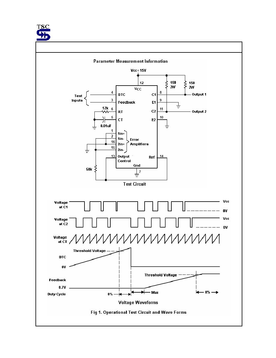
Vi (pin4)= 2V, See Figure 1
--
7.5
--
mA
SWITCHING CHARACTERISTICS
Output voltage rise time
--
100
200
Output voltage fall time
Common-emitter configuration,
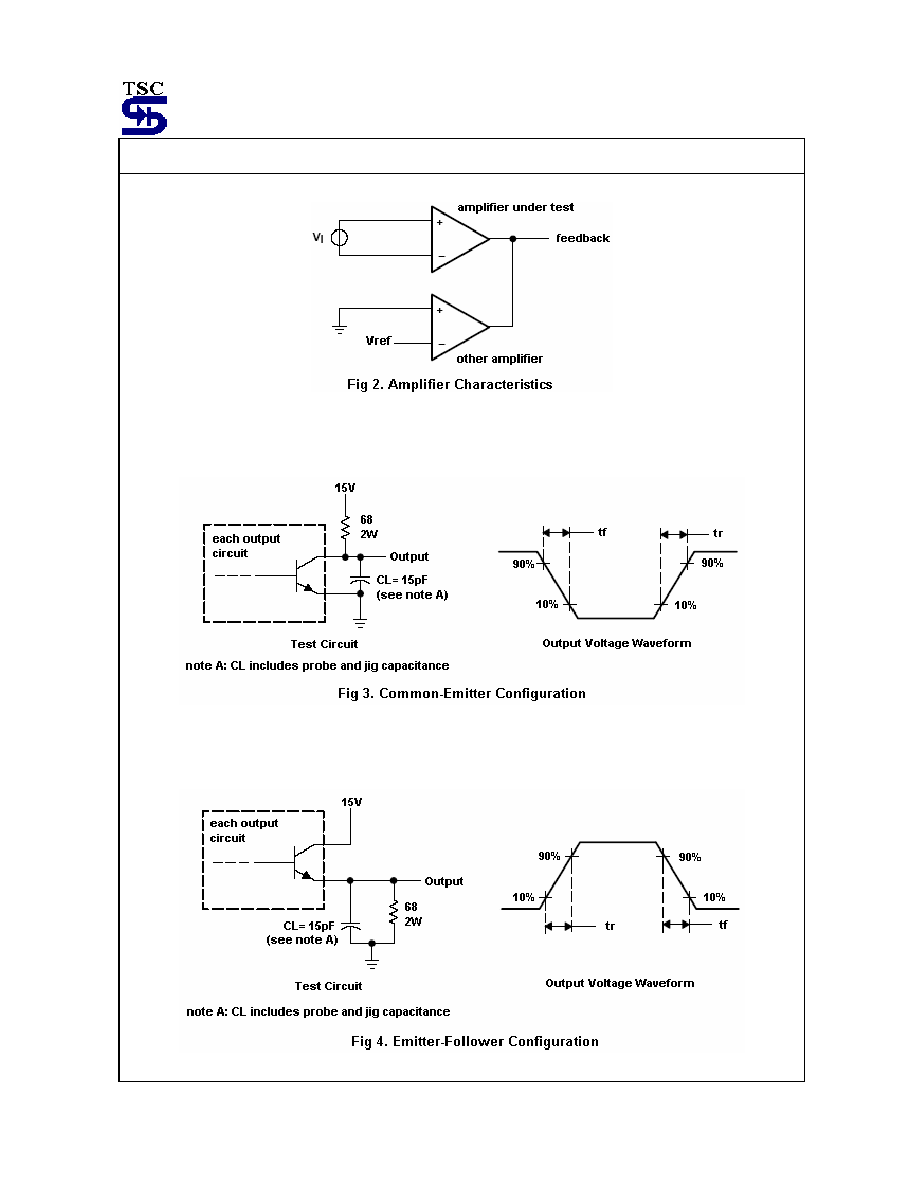
See Figure 3
-- 25 100
Output voltage rise time
--
100
200
Output voltage fall time
Emitter-follower configuration,
See Figure 4
-- 40 100
ns
UNDERVOLTAGE LOCKOUT SECTION
Turn-on Threshold
Vcc increasing Iref = 1.0mA
5.5
6.43
7.0
V
Remark:
All typical value except for temperature coefficient are at Ta= 25
o
C
For conditions shown as Min or Max, use the appropriate value specified under recommended operating
conditions.
All typical values except for parameter changes with temperature are at Ta= 25
o
C
Duration of the short-circuit should not exceed one second
Standard deviation is a measure of the statistical distribution about the mean as derived from the formula
2
1
1
2
1
)
(
-
-
=
=
N
n
n
N
x
x
Temperature coefficient of timing capacitor and timing resistor not taken into account
TS494 5-7
2003/12
rev.
A
Parameter Measurement Information
TS494 6-7
2003/12
rev.
A
Parameter Measurement Information (continues)
TS494 7-7
2003/12
rev.
A
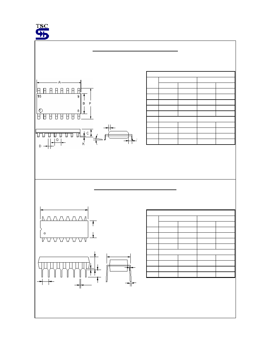
SOP-16 Mechanical Drawing
R
M
F
SOP-16 DIMENSION
MILLIMETERS INCHES
DIM
MIN MAX MIN MAX
A 9.80 10.00 0.386 0.393
B 3.80 4.00 0.150 0.157
C 1.35 1.75 0.054 0.068
D 0.35 0.49 0.014 0.019
F 0.40 1.25 0.016 0.049
G
1.27 (typ)
0.05 (typ)
K 0.10 0.25 0.004 0.009
M 0
o
7
o
0
o
7
o
P 5.80 6.20 0.229 0.244
R 0.25 0.50 0.010 0.019
DIP-16 Mechanical Drawing
D
G
K
C
N
A
1
16
B
8
9
L
M
J
SOP-16 DIMENSION
MILLIMETERS INCHES
DIM
MIN MAX MIN MAX
A 17.80 18.05 0.701 0.710
B 6.22 6.48 0.290 0.299
C 3.18 4.45 0.125 0.135
D 0.35 0.55 0.019 0.020
G
1.27 (typ)
0.05 (typ)
J 0.25 0.31 0.010 0.012
K 3.25 3.35 0.128 0.132
L 7.75 8.00 0.305 0.315
M - 10
o
- 10
o