TS5205 series
1-6
2004/09 rev. A
TS5205
150mA Low Noise LDO Voltage Regulator with Enable
Low Power Consumption
Low DropOut Voltage 0.275V
Fixed and Adjustable Output
Enable Shutdown
General Description
The TS5205 series is an efficient linear voltage regulator with ultra low noise output, very low dropout voltage (typically
17mV at light loads and 165mV at 150mA), and very low power consumption (600uA at 100mA), providing high output
current even when the application requires very low dropout voltage. The Chip Enable (CE) includes a CMOS or TTL
compatible input allows the output to be turned off to prolong battery life. When shutdown, power consumption drops
nearly to zero.
The TS5205 series is included a precision voltage reference, error correction circuit, a current limited output driver, over
temperature shutdown, revered battery protection and a reference bypass pin to improve its already excellent low-noise
performance.
The TS5205 series is available in fixed and adjustable output voltage version in 5-pin SOT-25 package.
Features
Ultra low noise output.
Output current up to 150mA
Low dropout voltage
Low power consumption
"Zero" off-mode current
Logic controlled electronic enable
Internal current limit and Thermal shutdown protection
Applications
Cellular telephones
Palmtops, notebook computers
Battery powered equipment
Consumer and personal electronics
SMPS post regulator and DC to DC modules
High-efficiency linear power supplies
Ordering Information
Note: Where xx denotes voltage option, available are
5.0V, 3.3V, 3.0V, 2.9V, 2.8V, 2.5V and 1.8V. Leave
blank for adjustable version. Contact factory for
additional voltage options.
Part No.
Operating Temp. Package
TS5205CX5xx
-40 ~ +125
o
C SOT-25
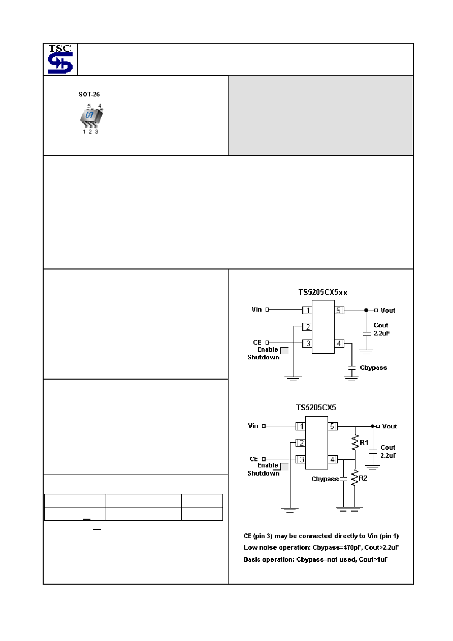
Typical Application Circuit
Pin assignment
1. Input
2. Ground
3. Enable
4. Bypass / Adjust
5. Output
TS5205 series
2-6
2004/09 rev. A
Absolute Maximum Rating
(Note 1)
Input Supply Voltage
Vin
-20~ +20
V
Enable Input Voltage
Vce
-20~ +20
V
Power Dissipation (Note 2)
P
D
Internal limited
Thermal Resistance
ja 220
o
C/W
Operating Junction Temperature Range
Tj
-40 ~ +125
o
C
Storage Temperature Range
T
STG
-65 ~ +150
o
C
Lead Soldering Temperature (260
o
C)
5
S
Recommend Operating Rating
(Note 3)
Input Supply Voltage
Vin
+2.5 ~ +16
V
Enable Input Voltage
Vce
0 ~ Vin
V
Electrical Characteristics
Vin=Vo+1V, Io=100uA, Cout=1uF, Vce
2V, Tj = 25
o
C, unless otherwise specified.
Parameter Conditions
Min
Typ
Max
Unit
Output Voltage
Vin=Vo + 1V
0.99|Vo| Vout 1.01|Vo| V
Output Voltage Temp. Coefficient (Note 4)
--
40
--
ppm/
o
C
Line Regulation
Vo+1V
Vin 16V
--
0.005
0.05
%/V
Load Regulation (Note 5)
0.1mA
Io 150mA
--
0.02
0.2
%/V
Io=100uA --
17
50
Io=50mA --
110
150
Io=100mA --
140
250
Dropout Voltage (Note 6)
Io=150mA --
165
275
mV
Quiescent Current
Vin
0.4V (shutdown)
Vin
0.18V (shutdown)
--
--
0.01
--
1
5
uA
Io=100uA --
80 125
Io=50mA -- 350 600
Io=100mA
-- 600
1000
Ground Pin Current (Note 7)
Vce
2V
Io=150mA
-- 1300
1900
uA
Output Current Limit
Vout=0V
--
300
500
mA
Power Supply Rejection Ratio
At f=100Hz, Io=100uA,
--
75
--
dB
Thermal Regulation (Note 8)
--
0.05
--
%/W
Output Noise
Io=50mA, Cout=2.2uF,
470pF from bypass to Ground
-- 260 --
nVHz
Enable function
Enable Input Logic-Low Voltage
Regulation shutdown
--
--
0.4
V
Enable Input Logic-High Voltage Regulation
enable
2.0
--
--
V
V
IL
0.4V
--
0.01
-1
Enable Input Current
V
IH
2.0
V --
5
20
uA
TS5205 series
3-6
2004/09 rev. A
Electrical Characteristics (continued)
Note 1: Exceeding the absolute maximum rating may damage the device.
Note 2: The maximum allowable power dissipation at any Ta is Pd(max) = [ Tj(max) - Ta] + ja. Exceeding the
maximum allowable power dissipation will result in excessive die temperature, and the regulator will go into
thermal shutdown.
Note 3: The device is not guaranteed to function outside its operating rating.
Note 4: Output voltage temperature coefficient is defined as the worst case voltage change divided by the total
temperature range.
Note 5: Regulation is measured at constant junction temperature using low duty cycle pulse testing. Parts are tested
for load regulation in the load range from 1mA to 150mA. Changes in output voltage due to heating effects
are covered by the thermal regulation specification.
Note 6: Dropout voltage is defined as the input to output differential at which the output voltage drops 2% below its
nominal value measured at 1V differential.
Note 7: Ground pin current is the regulator quiescent current plus pass transistor base current. The total current
drawn from the supply is the sum of the load current plus the ground pin current.
Note 8: Thermal regulation is defined as the change in output voltage at a time "t" after a change in power dissipation
is applied, excluding load or line regulation effects. Specifications are for a 150mA load pulse at Vin=16V for
t=10mS.
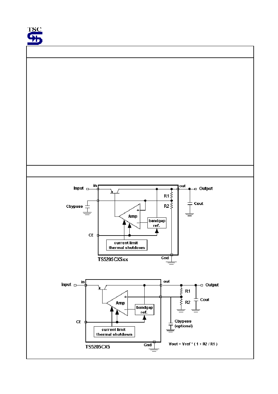
Block Diagrams
TS5205 series
4-6
2004/09 rev. A
Application Information
Enable Input
TS5205 series feature an active-high (>2V) enable (EN)
input that allows ON/OFF control of the regulator.
Current drain reduces to "zero" when the device is
shutdown, with only micro-amperes of leakage current.
The EN is compatible with CMOS logic interfacing. EN
may be directly tied to Vin and pulled up to the
maximum supply voltage.
Input Capacitor Requirement
An input capacitor of 1uF or greater is recommended
when the device is more than 10" away from the bulk
AC supply capacitance or when the supply is a battery.
Reference Bypass Capacitor
Bypass is connected to the internal voltage reference. A
470uF capacitor (Cbypass) connected from Bypass to
Ground quiets this reference, providing a significant
reduction in output noise. Cbypass reduces the
regulator phase margin; when using Cbypass, output
capacitors of 2.2uF or greater are generally required to
maintain stability.
The star up speed of the TS5205 is inversely
proportional to the size of the reference bypass
capacitor. Applications requiring a slow ramp up of
output voltage should consider larger values of
Cbypass. Likewise, if rapid turn on is necessary,
consider omitting Cbypass. If output noise is not a
major concern, omitted Cbypass and leave Bypass
open.
Output Capacitor Requirement
The TS5205 series requires an output capacitor to
maintain stability and improve transient response is
necessary. The value of this capacitor is dependent
upon whether a reference bypass capacitor is used.
1uF minimum is recommended when Cbypass is not
used. 2.2uF minimum is recommended when Cbypass
is 470uF. Larger values improve the regulator's
transient response. The output capacitor value may be
increased without limit.
The output capacitor should have an ESR (effective
series resistance) less than 5 and a resonant
frequency above 1MHz. Ultra low ESR capacitors can
cause a low amplitude oscillation on the output and/or
under damped transient response.
Most of tantalum or aluminum electrolytic capacitors
are adequate; film types will work. Since many
aluminum electrolytic have electrolytes that freeze at
about ≠30
o
C, solid tantalums are recommended for
operation below ≠25
o
C. At lower values of output
current, less output capacitance is required for output
stability. The capacitor can be reduced to 0.47uF for
current below 10mA or 0.33uF for currents below 1mA.
No Load Stability
The TS5205 series iwill remain stable and in regulation
with no load, unlike many other voltage regulators.
This is especially important in CMOS RAM keep alive
applications.
Adjustable Regulator Design
The adjustable regulator versions can be adjusted to a
specific output voltage by using two external resistors
to programming the output voltage anywhere between
1.25 and the 16V maximum operating rating of the
family.
Two resistors are used. Resistors can be quite large
up to 470k, because of the very high input
impedance and low bias current of the sense
comparator, the resistor values are calculated by:
Vout = 1.242V * (R2 / R1 + 1)
A capacitor from Adj to Ground provides greatly
improved noise performance.
Dual Supply Operation
When used in dual supply systems where the regulator
load is returned to a negative supply, the output
voltage must be diode clamped to ground.
TS5205 series
5-6
2004/09 rev. A
Application Information (continues)
Thermal Characteristics
TS5205 series is designed to provide 150mA of
continuous current in a very small package. Maximum
power dissipation can be calculated based on the
output current and the voltage drop across the part. To
determine the maximum power dissipation of the
package, use the junction-ambient thermal resistance
of the device and the following basic equation:
Pd(max) = [ Tj(max) ≠ Ta ] /ja
Tj(max) is the maximum junction temperature of the
die(125
o
C), and Ta is the ambient operating
temperature. ja is layout dependent, the actual power
dissipation of the regulator circuit can be determined
using the equation:
Pd = ( Vin ≠ Vout ) * Iout + Vin * Ignd
Substituting Pd(max) for Pd and solving for the
operating conditions that are critical to the application
will give the maximum operating conditions for the
regulator circuit. For example, when operating the
TS5205CX533 at room temperature with a minimum
footprint layout, the maximum input voltage for a set
output current can be determined as follows:
Pd(max) = (125
o
C ≠ 25
o
C) / 220
o
C/W
Pd(max) = 455mW
The junction to ambient thermal resistance for the
minimum footprint is 220
o
C/W, the maximum power
dissipation must not be exceeded for proper operation.
Using the output voltage of 3.3V and an output current
of 150mA, the maximum input voltage can be
determined. Formt eh electrical characteristics table,
the maximum ground current for 150mA output current
is 2.5mA.
445mW = ( Vin ≠ 3.3V ) * 150mA + Vin * 2.5mA
445mW = Vin * 150mA ≠ 3.3 * 150mA + Vin * 2.5mA
445mW = Vin * 150mA ≠ 495mW + Vin * 2.5mA
950mW = Vin * 152.5mA
Vin(max) = 6.23v
Therefore, a 3.3V application at 150mA of output
current can accept a maximum input voltage of 6.23V
in a SOT-25 package.
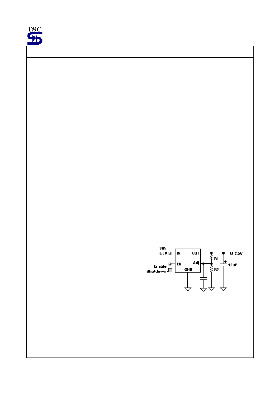
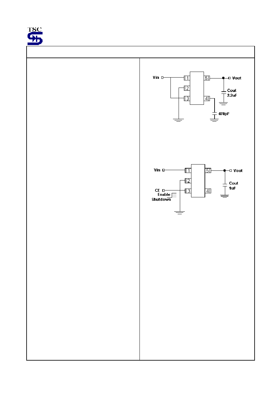
Fixed Output Regulator Application
Ultra Low Noise Fixed Voltage Application
Includes a 470uF capacitor for low noise operation and
shows EN connected to IN for an application where
enable/shutdown is not required. Cout= 2.2uF
minimum.
Low Noise Fixed Voltage Application
An example of a low noise configuration where Cbypass
is not required. Cout= 1uF minimum
TS5205 series
6-6
2004/09 rev. A
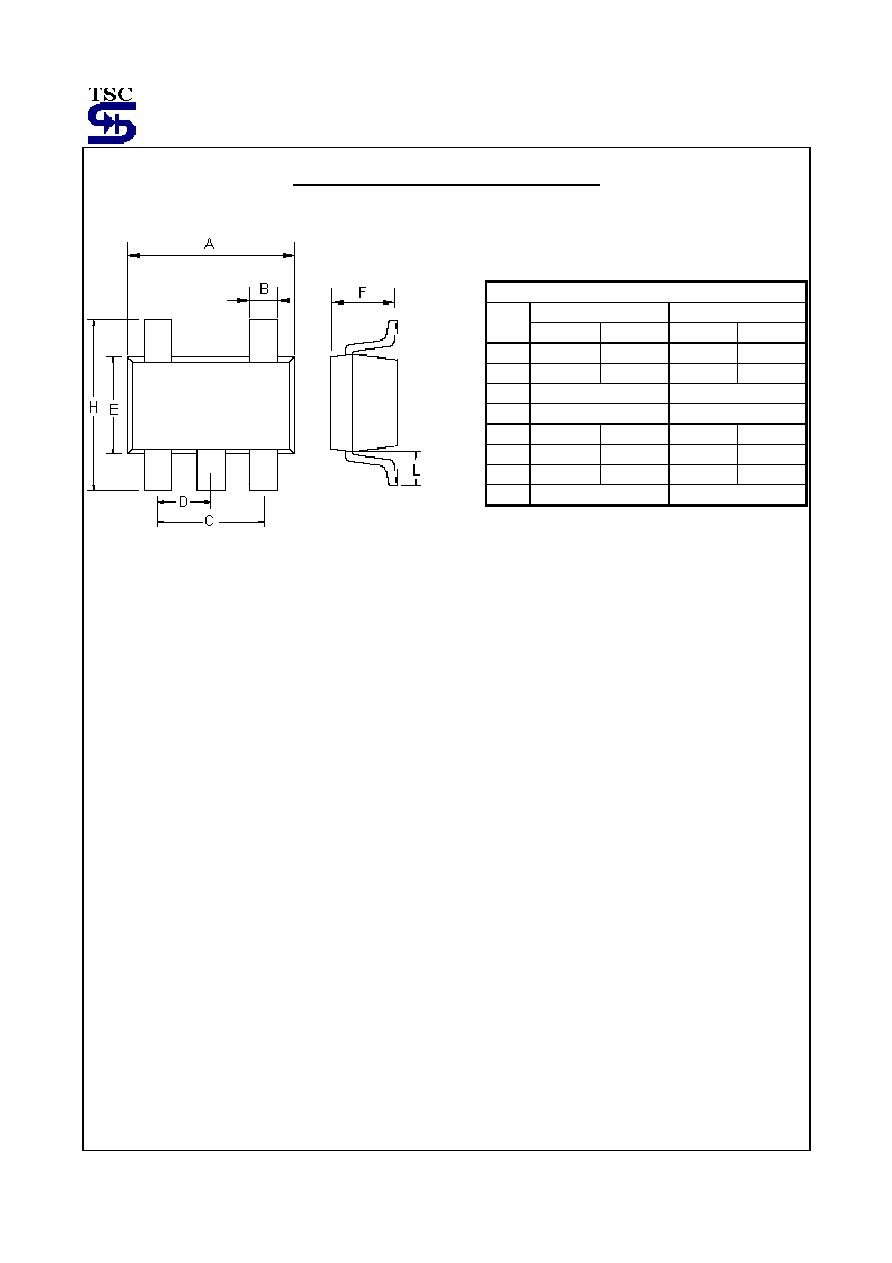
SOT-25 Mechanical Drawing
SOT-25 DIMENSION
MILLIMETERS INCHES
DIM
MIN MAX MIN MAX
A 2.70 3.00 0.106 0.118
B 0.25 0.50 0.010 0.020
C 1.90(typ)
0.075(typ)
D 0.95(typ)
0.037(typ)
E 1.50 1.70 0.059 0.067
F 1.05 1.35 0.041 0.053
H 2.60 3.00 0.102 0.118
L 0.60(typ)
0.024(typ)