
TS650 1-4
2003/12
rev.
A
TS650
Buck Switching Regulator
Pin assignment:
1. Out
2. P.Gnd
3. CT
4. Gnd
5. FB
6. Vcc
7. Comp.
8.
Enable
Supply Voltage Range 3 V to 30V
Output Driving Current 500mA
Oscillator Frequency up to 100KHz
General Description
The TS650 is a monolithic buck switching regulator, it is consist of an voltage reference, error amplifier, current limited set
by an external resistor, power forward modular controller and switching frequencies up to 100KHz are set by an external
capacitor.
Additionally, a chip enable feature is provided to power down reducing the supply current, and with a minimum number of
external components, the TS650 offer a simple and cost effective solution.
The TS650 is offered in SOP-8 package.
Features
Power forward control circuit
Operating voltage form 3V to 30V
Low
standby
current
Current limit adjustable
Output switch current up to 500mA
Variable oscillator frequency up to 100KHz (max)
Shut
down
control
1.25V voltage reference Output
Pin Descriptions
Name Description
Output PWM
Output
P.Gnd Power
Ground
CT Oscillator
Control
Gnd Ground
FB Voltage
Feedback
Vcc Power
Supply
Comp. Feedback
Compensation
Enable ON/OFF
control
Applications
Charger
xD-ROM, xDSL product
DC to DC converter s
Ordering Information
Part No.
Operating Temp.
Package
TS650CS -20
~
+85
o
C SOP-8
Block Diagram
TS650 2-4
2003/12
rev.
A
Absolute Maximum Rating
Supply Voltage
V
CC
30
V
Comparator Input Voltage Range
V
FB
- 0.3 ~ 30
V
Collector Output Voltage
V
C(SW)
30 V
Collector to Emitter Voltage
V
CE(SW)
30 V
Output Switching Current
I
SW
500 mA
Operating Junction Temperature Range
T
J
-20
~
+125
o
C
Storage Temperature Range
T
STG
-65
~
+150
o
C
Lead Temperature 1.6mm(1/16") from case for 10Sec.
T
LEAD
260
o
C
Electrical Characteristics
(V
CC
=5V, Ta =25
o
C; unless otherwise specified.)
Parameter Symbol
Test
Conditions Min
Typ
Max
Unit
Reference
Comp. Connect to FB
1.23 1.25 1.27 V
Ta= -20
o
C ~ 25
o
C
-
0.1
1
Output voltage change with
temperature
V
REF
Ta= 25
o
C ~ 85
o
C
-
0.2
1
%
Line regulation
RegLine
V
CC
= 5V ~ 30V
5
mV
Output switch (note1)
Saturation Voltage
V
CE(SAT)
I
SW
=0.5A
1.0
1.2 V
DC current gain
H
FE
I
SW
=1A, Vce=0.5V
75
--
Collector off-state current
I
C(OFF)
Vce=30V
40
100
uA
Oscillator (OSC)
Frequency F
OSC
C
T
=
1nF,
Vpin5=0V
24 33 42 KHz
Charge Current
I
CHARGE
V
CC
= 5V ~ 30V
35
uA
Discharge Current
I
DISCHARGE
V
CC
= 5V ~ 30V
220
uA
Discharge to Charge current ratio
I
DISCHARGE
/ I
CHARGE
Pin7 to Vcc
6.5
--
Current Limit Sense Voltage
V
IPK(SENSE)
I
DISCHARGE
= I
CHARGE
250 350
mV
ON/OFF driver control
ON
driver
voltage
Von
4 5 V
OFF driver voltage
Voff
1
V
ON driver current
Ion
V
CC
= 3V ~ 30V
100
mA
Total device
supply current
I
CC
V
CC
= 5V ~ 30V, C
T
= 1nF,
pin7=Vcc, pin5>Vth,
pin2=Gnd, remaining pins
open
3 5
mA
Input bias current
I
IB
Vin=0V
-400
nA
Note 1: Low duty cycle pulse techniques are used during test to maintain junction temperature as close to ambient
temperature.
TS650 3-4
2003/12
rev.
A
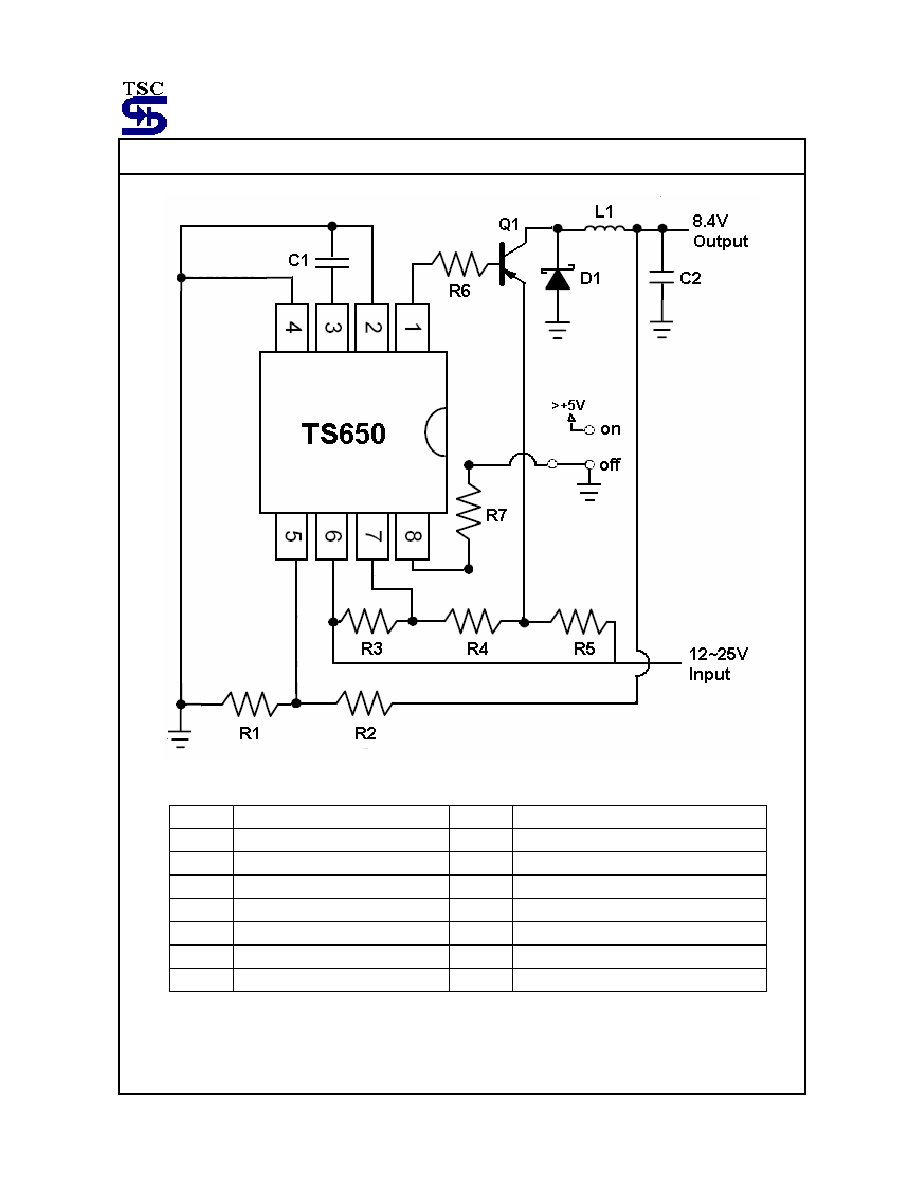
Typical Application Circuit
Device Value Device
Value
R1 5.6K,
1/8W C1
470pF,
16V
R2 1K,1/8W C2 470uF,
16V
R3
100ohm, 1/4W
L1
180uH, 2A
R4 100ohm,
1/4W D1
SK34A
R5 0.33ohm,
1W Q1
TSB1386CY
R6 300ohm,
1/2W
R7 300ohm,
1/2W
Remark:
* Output = 1.25V * (R1/R2 +1) = 1.25V * (5.6K/1K + 1) = 8.25V @ 3A
* SK34A: Taiwan semiconductor, Schottky 3A/40V in SMA package
* TSB1386CY: Taiwan semiconductor, PNP transistor 5A/20V in SOT-89 package
TS650 4-4
2003/12
rev.
A
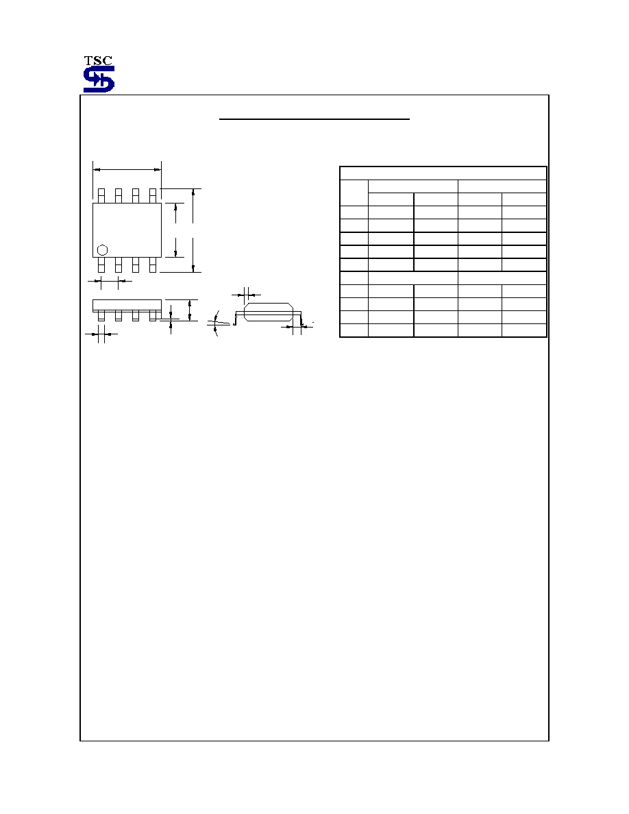
SOP-8 Mechanical Drawing
C
P
B
D
K
G
1
8
A
16
9
R
M
F
SOP-8 DIMENSION
MILLIMETERS INCHES
DIM
MIN MAX MIN MAX
A 4.80 5.00 0.189 0.196
B 3.80 4.00 0.150 0.157
C 1.35 1.75 0.054 0.068
D 0.35 0.49 0.014 0.019
F 0.40 1.25 0.016 0.049
G
1.27 (typ)
0.05 (typ)
K 0.10 0.25 0.004 0.009
M 0
o
7
o
0
o
7
o
P 5.80 6.20 0.229 0.244
R 0.25 0.50 0.010 0.019