TS7800I series
1-8
2003/12 rev. A
TS7800I series
3-Terminal Fixed Positive Voltage Regulator
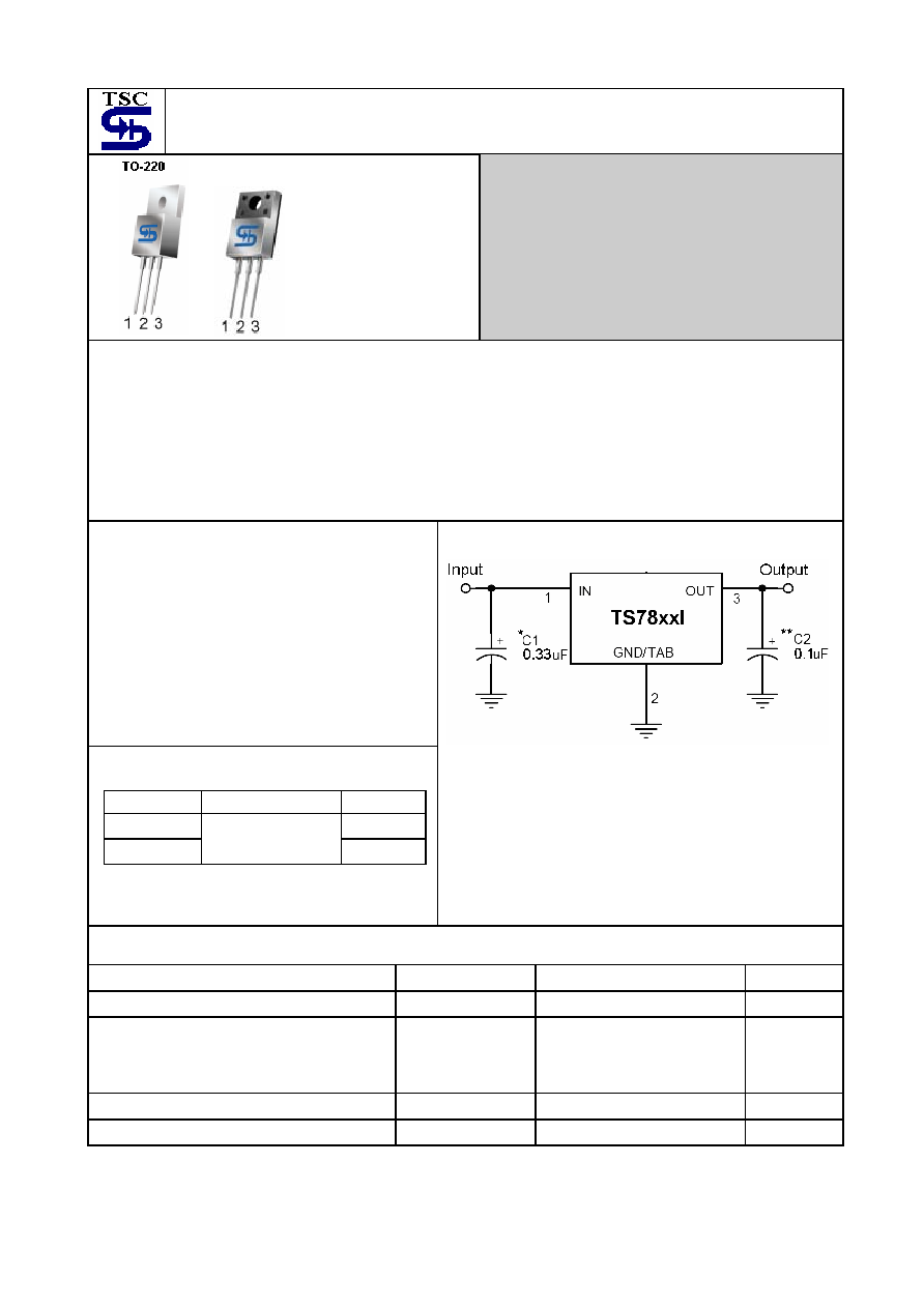
Pin assignment:
1. Input
2. Ground
3.
Output
(Heatsink surface
connected to Pin 2)
Voltage Range 5V to 24V
Output Current up to 1.5A
General Description
These voltage regulators are monolithic integrated circuits designed as fixed-voltage regulators for a wide variety of
applications including local, on-card regulation. These regulators employ internal current limiting, thermal shutdown, and
safe-area compensation. With adequate heatsink they can deliver output currents up to 1.5 ampere.
Although designed primarily as a fixed voltage regulator, these devices can be used with external components to obtain
adjustable voltages and currents.
This series is offered in 3-pin TO-220, ITO-220 package.
Features
Output current up to 1.5A
No external components required
Internal thermal overload protection
Internal short-circuit current limiting
Output transistor safe-area compensation
Output voltage offered in 2% tolerance
Ordering Information
Note: Where xx denotes voltage option.
Part No.
Operating Temp. Package
TS78xxICZ TO-220
TS78xxICI
-40 ~ +85
o
C
ITO-220
Standard Application
A common ground is required between the input and the
output voltages. The input voltage must remain typically 2.0V
above the output voltage even during the low point on the
Input ripple voltage.
XX = these two digits of the type number indicate voltage.
* = Cin is required if regulator is located an appreciable
distance from power supply filter.
** = Co is not needed for stability; however, it does improve
transient response.
Absolute Maximum Rating
Input Voltage
Vin *
35
V
Input Voltage
Vin **
40
V
Power Dissipation TO-220
TO-220
ITO-220
Without heatsink
Pt ***
Without heatsink
2
15
10
W
Operating Junction Temperature Range
T
J
0 ~ +125
o
C
Storage Temperature Range
T
STG
-65 ~ +150
o
C
Note : * TS7805 to TS7818
** TS7824
*** Follow the derating curve
ITO-220
TS7800I series
2-8
2003/12 rev. A
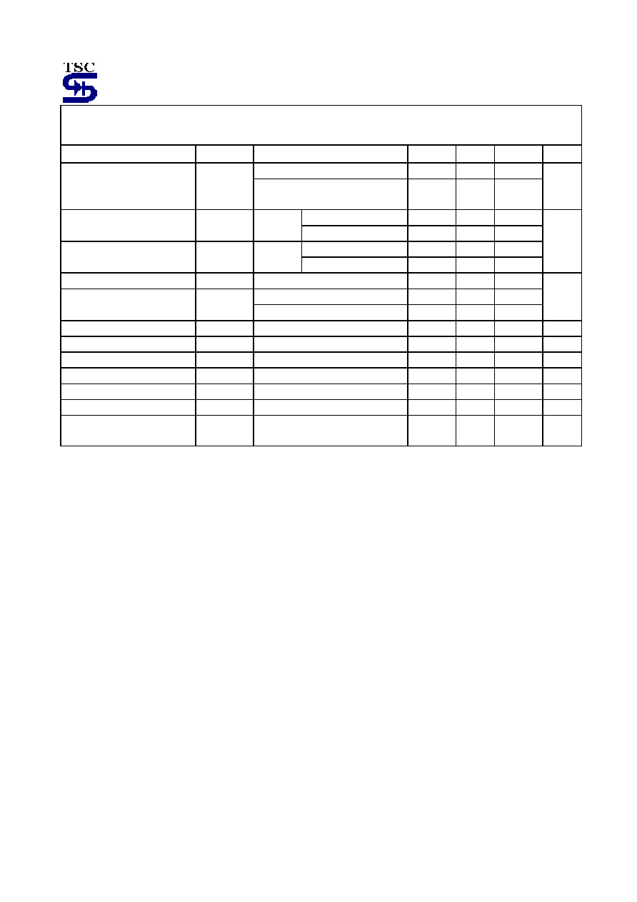
TS7805I Electrical Characteristics
(Vin=10V, Iout=500mA, 0
o
C
Tj125
o
C, Cin=0.33uF, Cout=0.1uF; unless otherwise specified.)
Parameter Symbol Test
Conditions Min
Typ
Max
Unit
Tj=25
o
C
4.90 5 5.10
Output voltage
Vout
7.5V
Vin20V, 10mAIout1.5A,
PD
15W
4.80 5 5.20
V
7.5V
Vin25V --
3
100
Line Regulation
REGline
Tj=25
o
C
8V
Vin12V --
1
50
10mA
Iout1.5A --
15
100
Load Regulation
REGload
Tj=25
o
C
250mA
Iout750mA
-- 5 50
mV
Quiescent Current
Iq
Iout=0, Tj=25
o
C --
4.2
8
7.5V
Vin25V --
--
1.3
Quiescent Current Change
Iq
10mA
Iout1.5A --
--
0.5
mA
Output Noise Voltage
Vn
10Hz
f100KHz, Tj=25
o
C
-- 40 -- uV
Ripple Rejection Ratio
RR
f=120Hz, 8V
Vin18V
62
78
--
dB
Voltage Drop
Vdrop
Iout=1.0A, Tj=25
o
C --
2
--
V
Output
Resistance
Rout
f=1KHz
-- 17 -- m
Output Short Circuit Current
Ios
Tj=25
o
C --
750
--
mA
Peak Output Current
Io peak
Tj=25
o
C
-- 2.2 -- A
Temperature Coefficient of
Output Voltage
Vout/ Tj Iout=10mA,
0
o
C
Tj125
o
C
-- -0.6 --
mV/
o
C
TS7806I Electrical Characteristics
(Vin=11V, Iout=500mA, 0
o
C
Tj125
o
C, Cin=0.33uF, Cout=0.1uF; unless otherwise specified.)
Parameter Symbol Test
Conditions Min
Typ
Max
Unit
Tj=25
o
C
5.88 6 6.12
Output Voltage
Vout
8.5V
Vin21V, 10mAIout1.5A,
PD
15W
5.76 6 6.24
V
8.5V
Vin25V --
5
120
Line Regulation
REGline
Tj=25
o
C
9V
Vin13V --
1.5
60
10mA
Iout1.5A --
14
120
Load Regulation
REGload
Tj=25
o
C
250mA
Iout750mA -- 4 60
mV
Quiescent Current
Iq
Iout=0, Tj=25
o
C --
4.3
8
8.5V
Vin25V --
--
1.3
Quiescent Current Change
Iq
10mA
Iout1.5A --
--
0.5
mA
Output Noise Voltage
Vn
10Hz
f100KHz, Tj=25
o
C
-- 45 -- uV
Ripple Rejection Ratio
RR
f=120Hz, 9V
Vin19V 59
75
--
dB
Voltage Drop
Vdrop
Iout=1.0A, Tj=25
o
C --
2
--
V
Output
Resistance
Rout
f=1KHz
-- 19 -- m
Output Short Circuit Current
Ios
Tj=25
o
C --
550
--
mA
Peak Output Current
Io peak
Tj=25
o
C
-- 2.2 -- A
Temperature Coefficient of
Output Voltage
Vout/ Tj Iout=10mA,
0
o
C
Tj125
o
C
-- -0.7 --
mV/
o
C
Pulse testing techniques are used to maintain the junction temperature as close to the ambient temperature as
possible, and thermal effects must be taken into account separately.
This specification applies only for DC power dissipation permitted by absolute maximum ratings.
TS7800I series
3-8
2003/12 rev. A
TS7808I Electrical Characteristics
(Vin=14V, Iout=500mA, 0
o
C
Tj125
o
C, Cin=0.33uF, Cout=0.1uF; unless otherwise specified.)
Parameter Symbol Test
Conditions Min
Typ
Max
Unit
Tj=25
o
C
7.84 8 8.16
Output Voltage
Vout
10.5V
Vin23V,
10mA
Iout1.5A, PD15W
7.68 8 8.32
V
10.5V
Vin25V --
6
160
Line Regulation
REGline
Tj=25
o
C
11V
Vin17V --
2
80
10mA
Iout1.5A --
12
160
Load Regulation
REGload
Tj=25
o
C
250mA
Iout750mA -- 4 80
mV
Quiescent Current
Iq
Iout=0, Tj=25
o
C --
4.3
8
10.5V
Vin25V --
--
1
Quiescent Current Change
Iq
10mA
Iout1.5A --
--
0.5
mA
Output Noise Voltage
Vn
10Hz
f100KHz, Tj=25
o
C
-- 52 -- uV
Ripple Rejection Ratio
RR
f=120Hz, 11V
Vin21V 56
72
--
dB
Voltage Drop
Vdrop
Iout=1.0A, Tj=25
o
C --
2
--
V
Output
Resistance
Rout
f=1KHz
-- 16 -- m
Output Short Circuit Current
Ios
Tj=25
o
C --
450
--
mA
Peak Output Current
Io peak
Tj=25
o
C
-- 2.2 -- A
Temperature Coefficient of
Output Voltage
Vout/ Tj Iout=10mA,
0
o
C
Tj125
o
C
-- -0.8 --
mV/
o
C
TS7809I Electrical Characteristics
(Vin=15V, Iout=500mA, 0
o
C
Tj125
o
C, Cin=0.33uF, Cout=0.1uF; unless otherwise specified.)
Parameter Symbol Test
Conditions Min
Typ
Max
Unit
Tj=25
o
C
8.82 9 9.18
Output Voltage
Vout
11.5V
Vin23V,
10mA
Iout1.5A, PD15W
8.64 9 9.36
V
11.5V
Vin26V --
6
180
Line Regulation
REGline
Tj=25
o
C
12V
Vin17V --
2
90
10mA
Iout1.5A --
12
180
Load Regulation
REGload
Tj=25
o
C
250mA
Iout750mA -- 4 90
mV
Quiescent Current
Iq
Iout=0, Tj=25
o
C --
4.3
8
11.5V
Vin26V --
--
1
Quiescent Current Change
Iq
10mA
Iout1.5A --
--
0.5
mA
Output Noise Voltage
Vn
10Hz
f100KHz, Tj=25
o
C
-- 52 -- uV
Ripple Rejection Ratio
RR
f=120Hz, 12V
Vin22V 55
72
--
dB
Voltage Drop
Vdrop
Iout=1.0A, Tj=25
o
C --
2
--
V
Output
Resistance
Rout
f=1KHz
-- 16 -- m
Output Short Circuit Current
Ios
Tj=25
o
C --
450
--
mA
Peak Output Current
Io peak
Tj=25
o
C
-- 2.2 -- A
Temperature Coefficient of
Output Voltage
Vout/ Tj Iout=10mA,
0
o
C
Tj125
o
C --
-1
--
mV/
o
C
Pulse testing techniques are used to maintain the junction temperature as close to the ambient temperature as
possible, and thermal effects must be taken into account separately.
This specification applies only for DC power dissipation permitted by absolute maximum ratings.

TS7800I series
4-8
2003/12 rev. A
TS7810I Electrical Characteristics
(Vin=16V, Iout=500mA, 0
o
C
Tj125
o
C, Cin=0.33uF, Cout=0.1uF; unless otherwise specified.)
Parameter Symbol Test
Conditions Min
Typ
Max
Unit
Tj=25
o
C 9.8
10
10.2
Output Voltage
Vout
12.5V
Vin25V,
10mA
Iout1.5A, PD15W
9.6 10 10.4
V
12.5V
Vin28V --
7
200
Line Regulation
REGline
Tj=25
o
C
13V
Vin17V --
2
100
10mA
Iout1.5A --
12
200
Load Regulation
REGload
Tj=25
o
C
250mA
Iout750mA -- 4 100
mV
Quiescent Current
Iq
Iout=0, Tj=25
o
C --
4.3
8
12.5V
Vin28V --
--
1
Quiescent Current Change
Iq
10mA
Iout1.5A --
--
0.5
mA
Output Noise Voltage
Vn
10Hz
f100KHz, Tj=25
o
C
-- 70 -- uV
Ripple Rejection Ratio
RR
f=120Hz, 13V
Vin23V 55
71
--
dB
Voltage Drop
Vdrop
Iout=1.0A, Tj=25
o
C --
2
--
V
Output
Resistance
Rout
f=1KHz
-- 18 -- m
Output Short Circuit Current
Ios
Tj=25
o
C --
400
--
mA
Peak Output Current
Io peak
Tj=25
o
C
-- 2.2 -- A
Temperature Coefficient of
Output Voltage
Vout/ Tj Iout=10mA,
0
o
C
Tj125
o
C --
-1
--
mV/
o
C
TS7812I Electrical Characteristics
(Vin=19V, Iout=500mA, 0
o
C
Tj125
o
C, Cin=0.33uF, Cout=0.1uF; unless otherwise specified.)
Parameter Symbol Test
Conditions Min
Typ
Max
Unit
Tj=25
o
C
11.76 12 12.24
Output Voltage
Vout
14.5V
Vin27V,
10mA
Iout1.5A, PD 15W
11.52 12 12.48
V
14.5V
Vin30V --
10
240
Line Regulation
REGline
Tj=25
o
C
15V
Vin19V --
3
120
10mA
Iout1.5A --
12
240
Load Regulation
REGload
Tj=25
o
C
250mA
Iout750mA -- 4 120
mV
Quiescent Current
Iq
Tj=25
o
C, Iout=0
--
4.3
8
14.5V
Vin30V --
--
1
Quiescent Current Change
Iq
10mA
Iout1.5A --
--
0.5
mA
Output Noise Voltage
Vn
10Hz
f100KHz, Tj=25
o
C
-- 75 -- uV
Ripple Rejection Ratio
RR
f=120Hz, 15V
Vin25V 55
71
--
dB
Voltage Drop
Vdrop
Iout=1.0A, Tj=25
o
C --
2
--
V
Output
Resistance
Rout
f=1KHz
-- 18 -- m
Output Short Circuit Current
Ios
Tj=25
o
C --
350
--
mA
Peak Output Current
Io peak
Tj=25
o
C
-- 2.2 -- A
Temperature Coefficient of
Output Voltage
Vout/ Tj Iout=10mA,
0
o
C
Tj125
o
C --
-1
--
mV/
o
C
Pulse testing techniques are used to maintain the junction temperature as close to the ambient temperature as
possible, and thermal effects must be taken into account separately.
This specification applies only for DC power dissipation permitted by absolute maximum ratings.
TS7800I series
5-8
2003/12 rev. A
TS7815I Electrical Characteristics
(Vin=23V, Iout=500mA, 0
o
C
Tj125
o
C, Cin=0.33uF, Cout=0.1uF; unless otherwise specified.)
Parameter Symbol Test
Conditions Min
Typ
Max
Unit
Tj=25
o
C
14.70 15 15.30
Output Voltage
Vout
17.5V
Vin30V,
10mA
Iout1.5A, PD 15W
14.40 15 15.60
V
17.5V
Vin30V --
12
300
Line Regulation
REGline
Tj=25
o
C
18V
Vin22V --
3
150
10mA
Iout1.5A --
12
300
Load Regulation
REGload
Tj=25
o
C
250mA
Iout750mA -- 4 150
mV
Quiescent Current
Iq
Tj=25
o
C, Iout=0
--
4.3
8
17.5V
Vin30V --
--
1
Quiescent Current Change
Iq
10mA
Iout1.5A --
--
0.5
mA
Output Noise Voltage
Vn
10Hz
f100KHz, Tj=25
o
C
-- 90 -- uV
Ripple Rejection Ratio
RR
f=120Hz, 18V
Vin28V 54
70
--
dB
Voltage Drop
Vdrop
Iout=1.0A, Tj=25
o
C --
2
--
V
Output
Resistance
Rout
f=1KHz
-- 19 -- m
Output Short Circuit Current
Ios
Tj=25
o
C --
230
--
mA
Peak Output Current
Io peak
Tj=25
o
C
-- 2.2 -- A
Temperature Coefficient of
Output Voltage
Vout/ Tj Iout=10mA,
0
o
C
Tj125
o
C --
-1
--
mV/
o
C
TS7818I Electrical Characteristics
(Vin=27V, Iout=500mA, 0
o
C
Tj125
o
C, Cin=0.33uF, Cout=0.1uF; unless otherwise specified.)
Parameter Symbol Test
Conditions Min
Typ
Max
Unit
Tj=25
o
C
17.64 18 18.36
Output Voltage
Vout
21V
Vin33V, 10mAIout1.5A,
PD
15W
17.28 18 18.72
V
21V
Vin33V --
15
360
Line Regulation
REGline
Tj=25
o
C
22V
Vin26V --
5
180
10mA
Iout1.5A --
12
360
Load Regulation
REGload
Tj=25
o
C
250mA
Iout750mA -- 4 180
mV
Quiescent Current
Iq
Tj=25
o
C, Iout=0
--
4.5
8
21V
Vin33V --
--
1
Quiescent Current Change
Iq
10mA
Iout1.5A --
--
0.5
mA
Output Noise Voltage
Vn
10Hz
f100KHz, Tj=25
o
C --
110
--
uV
Ripple Rejection Ratio
RR
f=120Hz, 21V
Vin31V 54
70
--
dB
Voltage Drop
Vdrop
Iout=1.0A, Tj=25
o
C --
2
--
V
Output
Resistance
Rout
f=1KHz
-- 22 -- m
Output Short Circuit Current
Ios
Tj=25
o
C --
200
--
mA
Peak Output Current
Io peak
Tj=25
o
C
-- 2.2 -- A
Temperature Coefficient of
Output Voltage
Vout/ Tj Iout=10mA,
0
o
C
Tj125
o
C --
-1
--
mV/
o
C
Pulse testing techniques are used to maintain the junction temperature as close to the ambient temperature as
possible, and thermal effects must be taken into account separately.
This specification applies only for DC power dissipation permitted by absolute maximum ratings.
TS7800I series
6-8
2003/12 rev. A
TS7824I Electrical Characteristics
(Vin=33V, Iout=500mA, 0
o
C
Tj125
o
C, Cin=0.33uF, Cout=0.1uF; unless otherwise specified.)
Parameter Symbol Test
Conditions Min
Typ
Max
Unit
Tj=25
o
C
23.52 24 24.48
Output Voltage
Vout
27V
Vin38V, 10mAIout1.5A,
PD
15W
23.04 24 24.96
V
27V
Vin38V --
18
480
Line Regulation
REGline
Tj=25
o
C
28V
Vin32V --
6
240
10mA
Iout1.5A --
12
480
Load Regulation
REGload
Tj=25
o
C
250mA
Iout750mA -- 4 240
mV
Quiescent Current
Iq
Iout=0, Tj=25
o
C --
4.6
8
27V
Vin38V --
--
1
Quiescent Current Change
Iq
10mA
Iout1.5A --
--
0.5
mA
Output Noise Voltage
Vn
10Hz
f100KHz, Tj=25
o
C --
170
--
uV
Ripple Rejection Ratio
RR
f=120Hz, 27V
Vin37V 54
70
--
dB
Voltage Drop
Vdrop
Iout=1.0A, Tj=25
o
C --
2
--
V
Output
Resistance
Rout
f=1KHz
-- 28 -- m
Output Short Circuit Current
Ios
Tj=25
o
C --
150
--
mA
Peak Output Current
Io peak
Tj=25
o
C
-- 2.2 -- A
Temperature Coefficient of
Output Voltage
Vout/ Tj Iout=10mA,
0
o
C
Tj125
o
C
-- -1.5 --
mV/
o
C
Pulse testing techniques are used to maintain the junction temperature as close to the ambient temperature as
possible, and thermal effects must be taken into account separately.
This specification applies only for DC power dissipation permitted by absolute maximum ratings.
TS7800I series
7-8
2003/12 rev. A
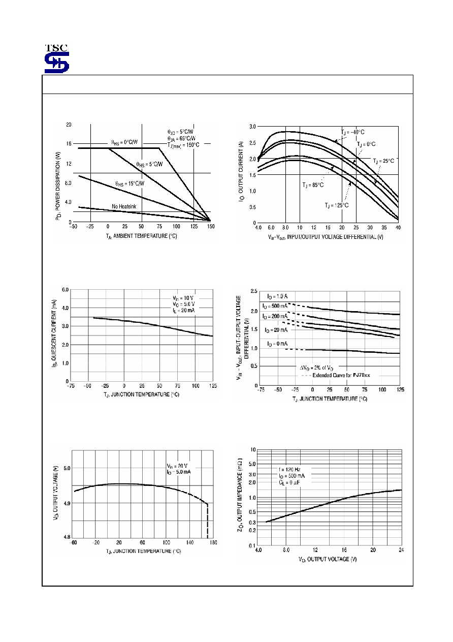
Electrical Characteristics Curve
FIGURE 1 - Worst Case Power Dissipation v.s.
Ambient Temperature
FIGURE 2 - Peak Output Current v.s.
Input-Output Differential Voltage
FIGURE 3 � Quiescent Current v.s.
Junction Temperature
FIGURE 4 � Input Output Differential v.s.
Junction Temperature
FIGURE 5 � Output Voltage v.s.
Junction Temperature
FIGURE 6 � Output Impedance v.s.
Output Voltage
TS7800I series
8-8
2003/12 rev. A
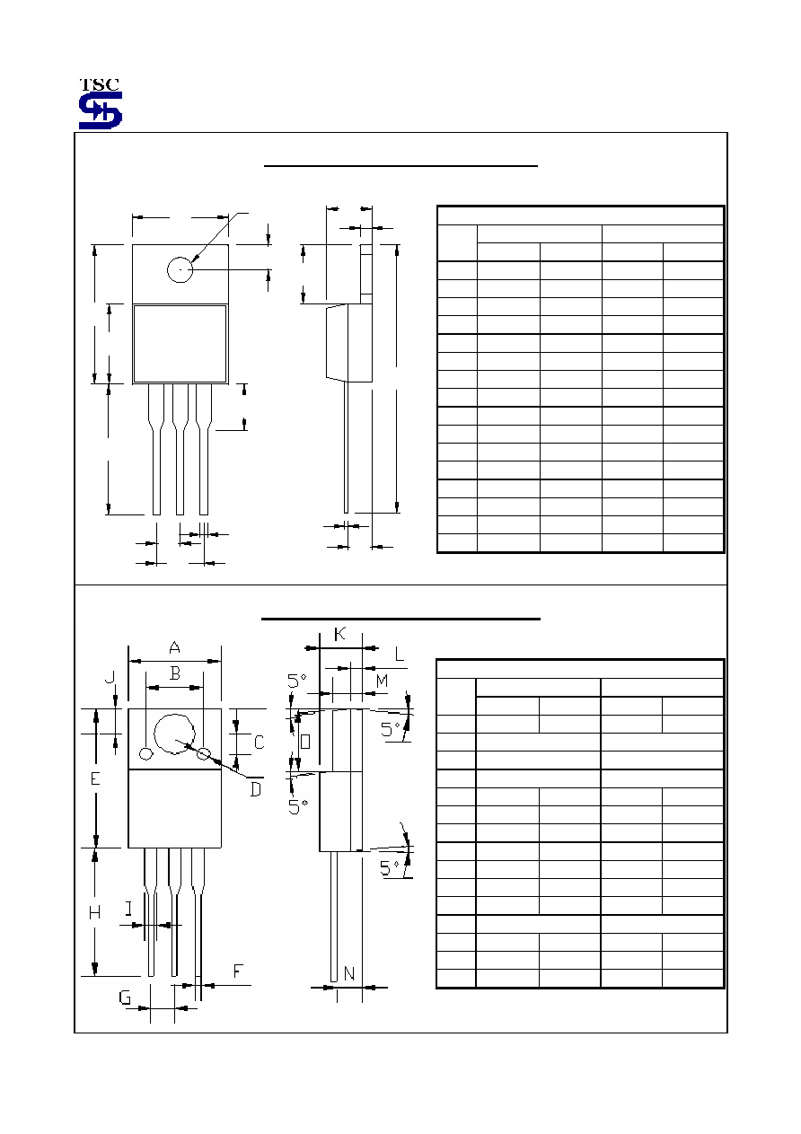
TO-220 Mechanical Drawing
I
J
H
E
G
F
D
C
B
A
M
N
O
L
K
P
TO-220 DIMENSION
MILLIMETERS INCHES
DIM
MIN MAX MIN MAX
A 10.000 10.500 0.394 0.413
B 3.240 4.440 0.128 0.175
C 2.440 2.940 0.096 0.116
D - 6.350 - 0.250
E 0.381 1.106 0.015 0.040
F 2.345 2.715 0.092 0.058
G 4.690 5.430 0.092 0.107
H 12.700 14.732 0.500 0.581
I 8.382 9.017 0.330 0.355
J 14.224 16.510 0.560 0.650
K 3.556 4.826 0.140 0.190
L 0.508 1.397 0.020 0.055
M 27.700 29.620 1.060 1.230
N 2.032 2.921 0.080 0.115
O 0.255 0.610 0.010 0.024
P 5.842 6.858 0.230 0.270
ITO-220 Mechanical Drawing
ITO-220 DIMENSION
MILLIMETERS INCHES
DIM
MIN MAX MIN MAX
A 10.04 10.07 0.395 0.396
B
6.20 (typ.)
0.244 (typ.)
C
2.20 (typ.)
0.087 (typ.)
D
1.40 (typ.)
0.055 (typ.)
E 15.0 15.20 0.591 0.598
F 0.52 0.54 0.020 0.021
G 2.35 2.73 0.093 0.107
H 13.50 13.55 0.531 0.533
I 1.11 1.49 0.044 0.058
J 2.60 2.80 0.102 0.110
K 4.49 4.50 0.176 0.177
L
1.15 (typ.)
0.045 (typ.)
M 3.03 3.05 0.119 0.120
N 2.60 2.80 0.102 0.110
O 6.55 6.65 0.258 0.262