
TS78L00 series
1-8
2003/12 rev. B
TS78L00 series
3-Terminal Low Current Positive Voltage Regulator
Voltage Range 5V to 24V
Output Current up to 100mA
General Description
The TS78L00 Series of positive voltage Regulators are inexpensive, easy-to-use devices suitable for a multitude of
applications that require a regulated supply of up to 100mA. Like their higher power TS7800 and TS78M00 Series
cousins, these regulators feature internal current limiting and thermal shutdown making them remarkably rugged. No
external components are required with the TS78L00 devices in many applications.
These devices offer a substantial performance advantage over the traditional zener diode-resistor combination, as output
impedance and quiescent current are substantially reduced.
This series is offered in 3-pin TO-92, SOT-89 and 8-pin SOP-8 package.
Features
Output current up to 100mA
No external components required
Internal thermal overload protection
Internal short-circuit current limiting
Output transistor safe-area compensation
Output voltage offered in 4% tolerance
Ordering Information
Note: Where xx denotes voltage option.
Part No.
Operating Temp.
(Ambient)
Package
TS78LxxCT TO-92
TS78LxxCY SOT-89
TS78LxxACY SOT-89
TS78LxxCS
-20 ~ +85
o
C
SOP-8
Standard Application
A common ground is required between the input and the
output voltages. The input voltage must remain typically
2.0V above the output voltage even during the low point
on the Input ripple voltage.
XX = these two digits of the type number indicate voltage.
* = Cin is required if regulator is located an appreciable
distance from power supply filter.
** = Co is not needed for stability; however, it does
improve transient response.
Pin Assignment
Pin No.
TS78L00CT TS78L00ACY TS78L00CY TS78L00CS
Pin
Description
1 1 3 1
Output
2
2
2
2, 3, 6, 7
Ground
3 3 1 8
Input
4,
5
Non connected
TS78L00 series
2-8
2003/12 rev. B
Absolute Maximum Rating
Input Voltage
Vin *
35
V
Input Voltage
Vin **
40
V
Power Dissipation TO-92
TO-89
SOP-8
Pd
0.625
0.5
0.5
W
Operating Junction Temperature Range
T
J
0
~
+150
o
C
Storage Temperature Range
T
STG
-65
~
+150
o
C
Note : * TS78L05 to TS78L18
** TS78L24
TS78L05 Electrical Characteristics
(Vin=10V, Iout=40mA, 0
o
C
Tj125
o
C, Cin=0.33uF, Cout=0.1uF; unless otherwise specified.)
Parameter Symbol Test
Conditions Min
Typ
Max
Unit
Tj=25
o
C
4.80 5 5.20
Output voltage
Vout
7.5V
Vin20V,
5mA
Iout100mA
4.75 5 5.25 V
Line Regulation
REGline
Tj=25
o
C
7.5V
Vin20V,
Io=40mA
-- 50 150
5mA
Iout100mA --
20
60
Load Regulation
REGload
Tj=25
o
C
5mA
Iout40mA --
10
30
mV
Quiescent Current
Iq
Iout=0, Tj=25
o
C --
3
6
8V
Vin20V --
--
1.5
Quiescent Current Change
Iq
1mA
Iout40mA --
--
0.1
mA
Output Noise Voltage
Vn
10Hz
f100KHz, Tj=25
o
C
-- 40 -- uV
Ripple Rejection Ratio
RR
f=120Hz, 8V
Vin18V
41
49
--
dB
Voltage Drop
Vdrop
Tj=25
o
C
-- 1.7 -- V
Peak Output Current
Io peak
Tj=25
o
C --
0.15
--
A
Pulse testing techniques are used to maintain the junction temperature as close to the ambient temperature as
possible, and thermal effects must be taken into account separately.
This specification applies only for DC power dissipation permitted by absolute maximum ratings.
TS78L00 series
3-8
2003/12 rev. B
TS78L06 Electrical Characteristics
(Vin=11V, Iout=40mA, 0
o
C
Tj125
o
C, Cin=0.33uF, Cout=0.1uF; unless otherwise specified.)
Parameter Test
Conditions Min
Typ
Max
Unit
Tj=25
o
C
5.76 6 6.24
Output voltage
Vout
8.5V
Vin21V,
5mA
Iout100mA
5.70 6 6.30 V
Line Regulation
REGline
Tj=25
o
C
8.5V
Vin21V,
Io=40mA
-- 50 150
5mA
Iout100mA -- 20
60
Load Regulation
REGload
Tj=25
o
C
5mA
Iout40mA --
10
30
mV
Quiescent Current
Iq
Iout=0, Tj=25
o
C --
3
6
9V
Vin21V --
--
1.5
Quiescent Current Change
Iq
1mA
Iout40mA --
--
0.1
mA
Output Noise Voltage
Vn
10Hz
f100KHz, Tj=25
o
C
-- 40 -- uV
Ripple Rejection Ratio
RR
f=120Hz, 9V
Vin19V
41
49
--
dB
Voltage Drop
Vdrop
Tj=25
o
C
-- 1.7 -- V
Peak Output Current
Io peak
Tj=25
o
C --
0.15
--
A
TS78L08 Electrical Characteristics
(Vin=14V, Iout=40mA, 0
o
C
Tj125
o
C, Cin=0.33uF, Cout=0.1uF; unless otherwise specified.)
Parameter Symbol Test
Conditions Min
Typ
Max
Unit
Tj=25
o
C
7.69 8 8.32
Output Voltage
Vout
10.5V
Vin23V,
5mA
Iout100mA
7.61 8 8.40 V
Line Regulation
REGline
Tj=25
o
C
10.5V
Vin23V,
Io=40mA
-- 80 160
5mA
Iout100mA -- 25 80
Load Regulation
REGload
Tj=25
o
C
5mA
Iout40mA -- 10
40
mV
Quiescent Current
Iq
Iout=0, Tj=25
o
C --
3
6
11V
Vin23V --
--
1.5
Quiescent Current Change
lq
1mA
Iout40mA --
--
0.1
mA
Output Noise Voltage
Vn
10Hz
f100KHz, Tj=25
o
C
-- 60 -- uV
Ripple Rejection Ratio
RR
f=120Hz, 13V
Vin23V 37
57
--
dB
Voltage Drop
Vdrop
Tj=25
o
C
-- 1.7 -- V
Peak Output Current
Io peak
Tj=25
o
C --
0.15
--
A
Pulse testing techniques are used to maintain the junction temperature as close to the ambient temperature as
possible, and thermal effects must be taken into account separately.
This specification applies only for DC power dissipation permitted by absolute maximum ratings.
TS78L00 series
4-8
2003/12 rev. B
TS78L09 Electrical Characteristics
(Vin=15V, Iout=40mA, 0
o
C
Tj125
o
C, Cin=0.33uF, Cout=0.1uF; unless otherwise specified.)
Parameter Symbol Test
Conditions Min
Typ
Max
Unit
Tj=25
o
C
8.65 9 9.36
Output Voltage
Vout
11.5V
Vin24V,
5mA
Iout100mA
8.57 9 9.45 V
Line Regulation
REGline
Tj=25
o
C
11.5V
Vin24V,
Io=40mA
-- 90 180
5mA
Iout100mA -- 30 90
Load Regulation
REGload
Tj=25
o
C
5mA
Iout40mA -- 15
45
mV
Quiescent Current
Iq
Iout=0, Tj=25
o
C --
3
6
12V
Vin24V --
--
0.8
Quiescent Current Change
lq
5mA
Iout40mA --
--
0.5
mA
Output Noise Voltage
Vn
10Hz
f100KHz, Tj=25
o
C
-- 60 -- uV
Ripple Rejection Ratio
RR
f=120Hz, 14V
Vin24V 37
57
--
dB
Voltage Drop
Vdrop
Tj=25
o
C
-- 1.7 -- V
Peak Output Current
Io peak
Tj=25
o
C --
0.15
--
A
TS78L12 Electrical Characteristics
(Vin=19V, Iout=40mA, 0
o
C
Tj125
o
C, Cin=0.33uF, Cout=0.1uF; unless otherwise specified.)
Parameter Symbol Test
Conditions Min
Typ
Max
Unit
Tj=25
o
C
11.53 12 12.48
Output Voltage
Vout
14.5V
Vin27V,
5mA
Iout100mA
11.42 12 12.60 V
Line Regulation
REGline
Tj=25
o
C
14.5V
Vin27V,
Io=40mA
-- 120 240
mV
5mA
Iout100mA -- 40 120
Load Regulation
REGload
Tj=25
o
C
5mA
Iout40mA -- 20
60
Quiescent Current
Iq
Tj=25
o
C, Iout=0
--
3
6.5
16V
Vin27V --
--
1.5
Quiescent Current Change
lq
5mA
Iout40mA --
--
0.1
mA
Output Noise Voltage
Vn
10Hz
f100KHz, Tj=25
o
C
-- 80 -- uV
Ripple Rejection Ratio
RR
f=120Hz, 15V
Vin25V 37
42
--
dB
Voltage Drop
Vdrop
Tj=25
o
C
-- 1.7 -- V
Peak Output Current
Io peak
Tj=25
o
C --
0.15
--
A
Pulse testing techniques are used to maintain the junction temperature as close to the ambient temperature as
possible, and thermal effects must be taken into account separately.
This specification applies only for DC power dissipation permitted by absolute maximum ratings.

TS78L00 series
5-8
2003/12 rev. B
TS78L15 Electrical Characteristics
(Vin=23V, Iout=40mA, 0
o
C
Tj125
o
C, Cin=0.33uF, Cout=0.1uF; unless otherwise specified.)
Parameter Symbol Test
Conditions Min
Typ
Max
Unit
Tj=25
o
C
14.42 15 15.60
Output Voltage
Vout
17.5V
Vin30V,
5mA
Iout100mA
14.28 15 15.75 V
Line Regulation
REGline
Tj=25
o
C
17.5V
Vin30V,
Io=200mA
-- 150 300
mV
5mA
Iout100mA -- 50 150
Load Regulation
REGload
Tj=25
o
C
5mA
Iout40mA -- 25
75
Quiescent Current
Iq
Tj=25
o
C, Iout=0
--
3
6.5
20V
Vin30V --
--
1.5
Quiescent Current Change
lq
5mA
Iout40mA --
--
0.1
mA
Output Noise Voltage
Vn
10Hz
f100KHz, Tj=25
o
C
-- 90 -- uV
Ripple Rejection Ratio
RR
f=120Hz, 18V
Vin28V 34
39
--
dB
Voltage Drop
Vdrop
Tj=25
o
C
-- 1.7 -- V
Peak Output Current
Io peak
Tj=25
o
C --
0.15
--
A
TS78L18 Electrical Characteristics
(Vin=27V, Iout=40mA, 0
o
C
Tj125
o
C, Cin=0.33uF, Cout=0.1uF; unless otherwise specified.)
Parameter Symbol Test
Conditions Min
Typ
Max
Unit
Tj=25
o
C
17.30 18 18.72
Output Voltage
Vout
21V
Vin33V, 5mAIout100mA
17.14 18 18.90
V
Line Regulation
REGline
Tj=25
o
C
21V
Vin33V,
Io=40mA
-- 180 360
mV
5mA
Iout100mA -- 60 180
Load Regulation
REGload
Tj=25
o
C
5mA
Iout40mA -- 30
90
Quiescent Current
Iq
Tj=25
o
C, Iout=0
--
3
6.5
21V
Vin33V --
--
1.5
Quiescent Current Change
lq
5mA
Iout40mA --
--
0.1
mA
Output Noise Voltage
Vn
10Hz
f100KHz, Tj=25
o
C --
150
--
uV
Ripple Rejection Ratio
RR
f=120Hz, 23V
Vin33V 33
48
--
dB
Voltage Drop
Vdrop
Tj=25
o
C
-- 1.7 -- V
Peak Output Current
Io peak
Tj=25
o
C --
0.15
--
A
Pulse testing techniques are used to maintain the junction temperature as close to the ambient temperature as
possible, and thermal effects must be taken into account separately.
This specification applies only for DC power dissipation permitted by absolute maximum ratings.
TS78L00 series
6-8
2003/12 rev. B
TS78L24 Electrical Characteristics
(Vin=33V, Iout=40mA, 0
o
C
Tj125
o
C, Cin=0.33uF, Cout=0.1uF; unless otherwise specified.)
Parameter Symbol Test
Conditions Min
Typ
Max
Unit
Tj=25
o
C
23.07 24 24.96
Output Voltage
Vout
27V
Vin38V, 5mAIout100mA
22.85 24 25.20
V
Line Regulation
REGline
Tj=25
o
C
27V
Vin38V,
Io=40mA
-- 200 400
mV
5mA
Iout100mA -- 80 240
Load Regulation
REGload
Tj=25
o
C
5mA
Iout40mA -- 40
120
Quiescent Current
Iq
Iout=0, Tj=25
o
C --
4
7
28V
Vin38V --
--
1.5
Quiescent Current Change
lq
5mA
Iout40mA --
--
0.1
mA
Output Noise Voltage
Vn
10Hz
f100KHz, Tj=25
o
C --
200
--
uV
Ripple Rejection Ratio
RR
f=120Hz, 29V
Vin35V 31
45
--
dB
Voltage Drop
Vdrop
Tj=25
o
C
-- 1.7 -- V
Peak Output Current
Io peak
Tj=25
o
C --
0.15
--
A
Pulse testing techniques are used to maintain the junction temperature as close to the ambient temperature as
possible, and thermal effects must be taken into account separately.
This specification applies only for DC power dissipation permitted by absolute maximum ratings.
TS78L00 series
7-8
2003/12 rev. B
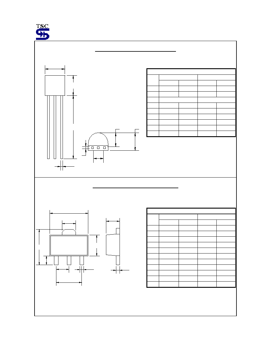
TO-92 Mechanical Drawing
C
D
A
B
H
E
F
G
TO-92 DIMENSION
MILLIMETERS INCHES
DIM
MIN MAX MIN MAX
A 4.30 4.70 0.169 0.185
B 4.30 4.70 0.169 0.185
C
14.30(typ)
0.563(typ)
D 0.43 0.49 0.017 0.019
E 2.19 2.81 0.086 0.111
F 3.30 3.70 0.130 0.146
G 2.42 2.66 0.095 0.105
H 0.37 0.43 0.015 0.017
SOT-89 Mechanical Drawing
SOT-89 DIMENSION
MILLIMETERS INCHES
DIM
MIN MAX MIN MAX
A 4.40 4.60 0.173 0.181
B 1.50 1.7 0.059 0.070
C 2.30 2.60 0.090 0.102
D 0.40 0.52 0.016 0.020
E 1.50 1.50 0.059 0.059
F 3.00 3.00 0.118 0.118
G 0.89 1.20 0.035 0.047
H 4.05 4.25 0.159 0.167
I 1.4 1.6 0.055
0.068
J 0.35 0.44 0.014 0.017
H
F
E
B
A
G
C
D
J
I

TS78L00 series
8-8
2003/12 rev. B
SOP-8 Mechanical Drawing
C
P
B
D
K
G
1
8
A
16
9
R
M
F
SOP-8 DIMENSION
MILLIMETERS INCHES
DIM
MIN MAX MIN MAX
A 4.80 5.00 0.189 0.196
B 3.80 4.00 0.150 0.157
C 1.35 1.75 0.054 0.068
D 0.35 0.49 0.014 0.019
F 0.40 1.25 0.016 0.049
G
1.27 (typ)
0.05 (typ)
K 0.10 0.25 0.004 0.009
M 0
o
7
o
0
o
7
o
P 5.80 6.20 0.229 0.244
R 0.25 0.50 0.010 0.019