
TSM1N60
1-4
2003/12 rev. E
TSM1N60
N-Channel Power Enhancement Mode MOSFET
V
DS
= 600V
I
D
= 1A
R
DS (on)
, Vgs @ 10V, Ids @ 0.6A = 8
General Description
The TSM1N60 is used an advanced termination scheme to provide enhanced voltage-blocking capability without
degrading performance over time. In addition, this advanced MOSFET is designed to withstand high energy in avalanche
and commutation modes. The new energy efficient design also offers a drain- to-source diode with a fast recovery time.
Designed for high voltage, high speed switching applications in power supplies, converters and PWM motor controls,
these devices are particularly well suited for bridge circuits where diode speed and commutating safe operating areas are
critical and offer additional and safety margin against unexpected voltage transients.
Features
Robust high voltage termination
Avalanche energy specified
Diode is characterized for use in bridge circuits
Source to Drain diode recovery time comparable to a
discrete fast recovery diode.
I
DSS
and V
DS(on)
specified at elevated temperature
Block Diagram
Ordering Information
Part No.
Packing
Package
TSM1N60CP
Tape & Reel
TO-252
TSM1N60CH Tube TO-251
Absolute Maximum Rating
(Ta = 25
o
C unless otherwise noted)
Parameter Symbol
Limit
Unit
Drain-Source Voltage
V
DS
600V V
Gate-Source Voltage
V
GS
�
30 V
Continuous Drain Current
I
D
1
A
Pulsed Drain Current
I
DM
9
A
Ta = 25
o
C 50
W
Maximum Power Dissipation
Ta > 25
o
C
P
D
0.4 W/
o
C
Operating Junction Temperature
T
J
+150
o
C
Operating Junction and Storage Temperature Range
T
J
, T
STG
- 55 to +150
o
C
Single Pulse Drain to Source Avalanche Energy
(V
DD
= 100V, V
GS
=10V, I
AS
=2A, L=10mH, R
G
=25)
E
AS
20
mJ
Thermal Performance
Parameter Symbol
Limit
Unit
Lead Temperature (1/8" from case)
T
L
10
S
Junction to Ambient Thermal Resistance (PCB mounted)
R
ja
62.5
o
C/W
Note: Surface mounted on FR4 board t<=10sec.
Pin assignment:
1. Gate
2. Drain
3. Source
TSM1N60
2-4
2003/12 rev. E
Electrical Characteristics
Tj = 25
o
C, unless otherwise noted
Parameter Conditions
Symbol
Min
Typ
Max
Unit
Static
Drain-Source Breakdown Voltage
V
GS
= 0V, I
D
= 250uA
BV
DSS
600 -- -- V
Drain-Source On-State Resistance
V
GS
= 10V, I
D
= 0.6A
R
DS(ON)
-- -- 8.0
Gate Threshold Voltage
V
DS
= V
GS
, I
D
= 250uA
V
GS(TH)
2.0 -- 4.0 V
Zero Gate Voltage Drain Current
V
DS
= 600V, V
GS
= 0V
I
DSS
-- -- 10
uA
Gate Body Leakage
V
GS
= � 20V, V
DS
= 0V
I
GSS
-- --
�
100
nA
Forward Transconductance
V
DS
50V, I
D
= 0.5A
g
fs
--
10
--
S
Dynamic
Total Gate Charge
Q
g
--
8.5
14
Gate-Source Charge
Q
gs
--
1.8
--
Gate-Drain Charge
V
DS
= 400V, I
D
= 1.0A,
V
GS
= 10V
Q
gd
-- 4 --
nC
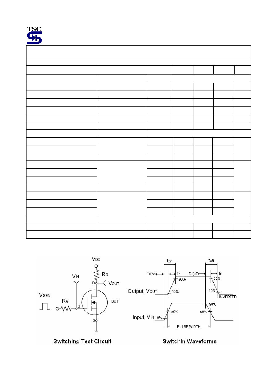
Turn-On Delay Time
t
d(on)
-- 8
Turn-On Rise Time
t
r
--
21
Turn-Off Delay Time
t
d(off)
-- 18
Turn-Off Fall Time
V
DD
= 300V, R
L
= 18,
I
D
= 1A, V
GEN
= 10V,
R
G
= 6
t
f
--
24
nS
Input Capacitance
C
iss
--
210
--
Output Capacitance
C
oss
--
28 --
Reverse Transfer Capacitance
V
DS
= 25V, V
GS
= 0V,
f = 1.0MHz
C
rss
--
4.2
--
pF
Source-Drain Diode
Max. Diode Forward Current
I
S
--
--
1.0
A
Diode Forward Voltage
I
S
= 1.0A, V
GS
= 0V
V
SD
-- --
1.5
V
Note: 1. pulse test: pulse width <=300uS, duty cycle <=2%
2. Negligible, Dominated by circuit inductance.
TSM1N60
4-4
2003/12 rev. E
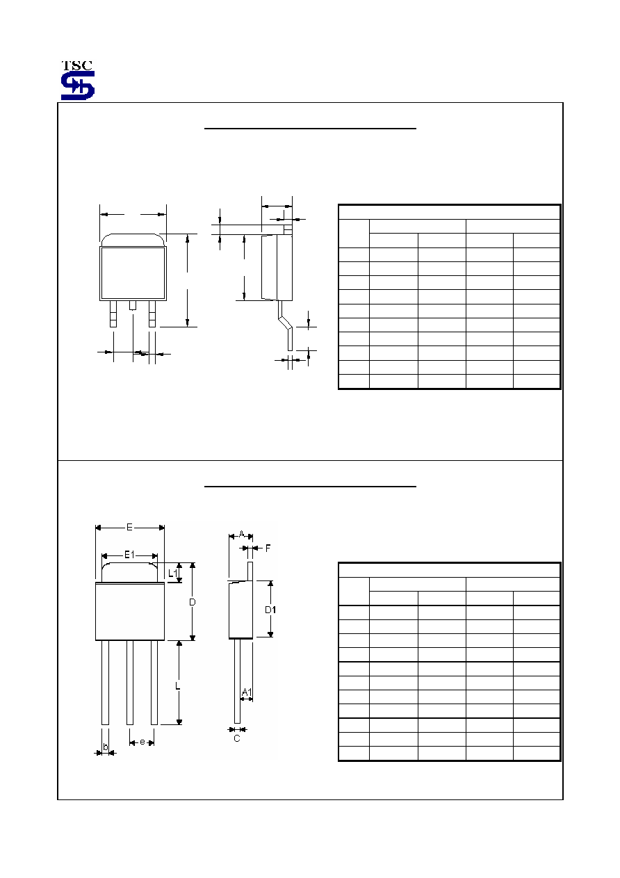
TO-252 Mechanical Drawing
B
C
D
A
F
G
I
H
E
J
TO-252 DIMENSION
MILLIMETERS INCHES
DIM
MIN MAX MIN MAX
A 6.570 6.840 0.259 0.269
B 9.250 10.400 0.364 0.409
C 0.550 0.700 0.022 0.028
D 2.560 2.670 0.101 0.105
E 2.300 2.390 0.090 0.094
F 0.490 0.570 0.019 0.022
G 1.460 1.580 0.057 0.062
H 0.520 0.570 0.020 0.022
I 5.340 5.550 0.210 0.219
J 1.460 1.640 0.057 0.065
TO-251 Mechanical Drawing
TO-251 DIMENSION
MILLIMETERS INCHES
DIM
MIN MAX MIN MAX
A 2.20 2.4 0.087 0.095
A1 1.10 1.30 0.043 0.051
b 0.40 0.80 0.016 0.032
C 0.40 0.60 0.016 0.024
D 6.70 7.30 0.264 0.287
D1
5.40 5.65 0.213
0.222
E 6.40 6.65 0.252 0.262
e 2.10 2.50 0.083 0.098
F 0.40 0.60 0.016 0.024
L 7.00 8.00 0.276 0.315
L1 1.60 1.86 0.063 0.073
