TSM2301
1-1
2003/12 rev. C
TSM2301
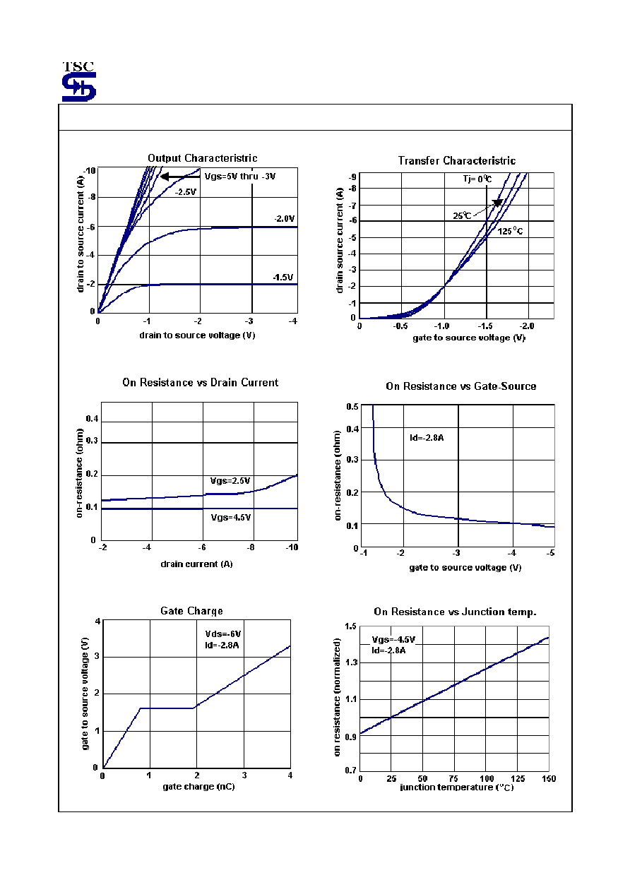
20V P-Channel Enhancement Mode MOSFET
V
DS
= - 20V
R
DS (on)
, Vgs @ - 4.5V, Ids @ - 2.8A =130m
R
DS (on)
, Vgs @ - 2.5V, Ids @ - 2.0A =190m
Features
Advanced trench process technology
High density cell design for ultra low on-resistance
Excellent thermal and electrical capabilities
Compact and low profile SOT-23 package
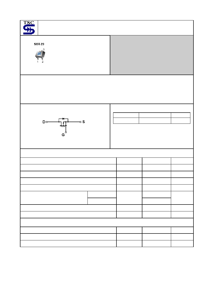
Block Diagram
Ordering Information
Part No.
Packing
Package
TSM2301CX
Tape & Reel
SOT-23
Absolute Maximum Rating
(Ta = 25
o
C
unless otherwise noted)
Parameter Symbol
Limit
Unit
Drain-Source Voltage
V
DS
-
20V V
Gate-Source Voltage
V
GS
�
8 V
Continuous Drain Current
I
D
- 2.3
A
Pulsed Drain Current
I
DM
-
10 A
Ta = 25
o
C 1.25
Maximum Power Dissipation
Ta = 75
o
C
P
D
0.8
W
Operating Junction Temperature
T
J
+150
o
C
Operating Junction and Storage Temperature Range
T
J
, T
STG
- 55 to +150
o
C
Thermal Performance
Parameter Symbol
Limit
Unit
Lead Temperature (1/8" from case)
T
L
5 S
Junction to Ambient Thermal Resistance (PCB mounted)
R
ja
100
o
C/W
Note: Surface mounted on FR4 board t<=5sec.
Pin assignment:
1. Gate
2. Source
3. Drain
TSM2301
2-2
2003/12 rev. C
Electrical Characteristics
Ta = 25
o
C, unless otherwise noted
Parameter Conditions
Symbol
Min
Typ
Max
Unit
Static
Drain-Source Breakdown Voltage
V
GS
= 0V, I
D
= - 250uA
BV
DSS
-
20 -- -- V
Drain-Source On-State Resistance
V
GS
= - 4.5V, I
D
= -2.8A
R
DS(ON)
-- 95 130
Drain-Source On-State Resistance
V
GS
= - 2.5V, I
D
= -2.0A
R
DS(ON)
-- 122
190
m
Gate Threshold Voltage
V
DS
= V
GS
, I
D
= - 250uA
V
GS(TH)
-
0.45 --
-- V
Zero Gate Voltage Drain Current
V
DS
= - 16V, V
GS
= 0V
I
DSS
-- --
-
1.0
uA
Gate Body Leakage
V
GS
= � 8V, V
DS
= 0V
I
GSS
-- --
�
100
nA
On-State Drain Current
V
DS
- 10V, V
GS
= -5V
I
D(ON)
-
6 -- -- A
Forward Transconductance
V
DS
= - 5V, I
D
= - 2.8A
g
fs
--
6.5
--
S
Dynamic
Total Gate Charge
Q
g
--
5.4
10
Gate-Source Charge
Q
gs
--
0.8
--
Gate-Drain Charge
V
DS
= - 6V, I
D
= - 2.8A,
V
GS
= - 4.5V
Q
gd
--
1.1
--
nC
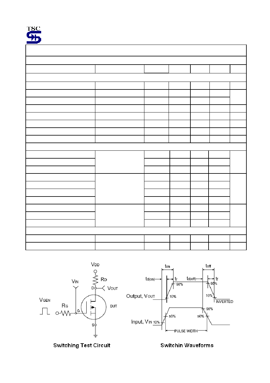
Turn-On Delay Time
t
d(on)
-- 5 25
Turn-On Rise Time
t
r
--
19
60
Turn-Off Delay Time
t
d(off)
-- 95
110
Turn-Off Fall Time
V
DD
= - 6V, R
L
= 6,
I
D
= - 1A, V
GEN
= - 4.5V,
R
G
= 6
t
f
--
65
80
nS
Input Capacitance
C
iss
--
447
--
Output Capacitance
C
oss
--
127
--
Reverse Transfer Capacitance
V
DS
= - 6V, V
GS
= 0V,
f = 1.0MHz
C
rss
--
80 --
pF
Source-Drain Diode
Max. Diode Forward Current
I
S
--
--
-
1.6
A
Diode Forward Voltage
I
S
= - 1.6A, V
GS
= 0V
V
SD
--
- 0.8
- 1.2
V
Note : pulse test: pulse width <=300uS, duty cycle <=2%
TSM2301
5-5
2003/12 rev. C
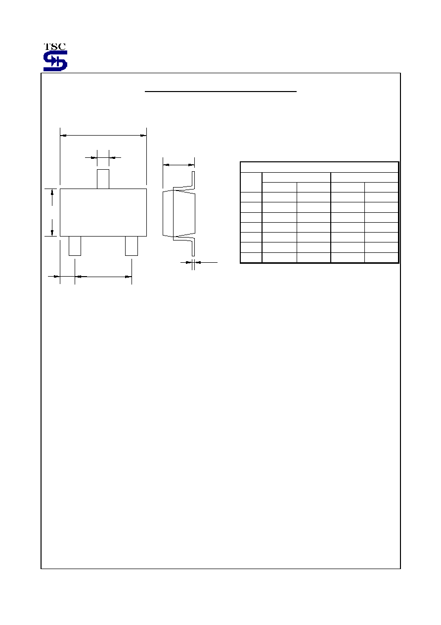
SOT-23 Mechanical Drawing
D
C
A
E
B
G
F
SOT-23 DIMENSION
MILLIMETERS INCHES
DIM
MIN MAX MIN MAX
A 2.88 2.91 0.113 0.115
B 0.39 0.42 0.015 0.017
C 1.78 2.03 0.070 0.080
D 0.51 0.61 0.020 0.024
E 1.59 1.66 0.063 0.065
F 1.04 1.08 0.041 0.043
G 0.07 0.09 0.003 0.004