TSM2N7000 1-3
2003/12
rev.
A
TSM2N7000
60V N-Channel Enhancement Mode MOSFET
V
DS
= 60V
I
D
= 200mA
R
DS (on)
, Vgs @ 10V, Ids @ 500mA = 5.0
General Description
The TSM2N7000 is produced using high cell density, DMOS technology. These products have been designed to
minimize on-state resistance while provide rugged, reliable and fast switching performance. It can be used in most
applications requiring up to 200mA DC and can deliver pulsed currents up to 500mA. This product is particularly suited
for low voltage, low current application such as small servo motor control, power MOSFET gate drivers, and other
switching applications.
Ordering Information
Part No.
Packing
Package
TSM2N7000CT A3
Ammo pack
TSM2N7000CT B0
Bulk pack
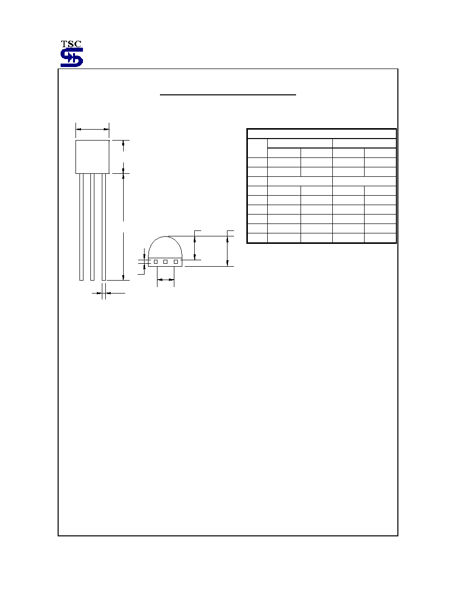
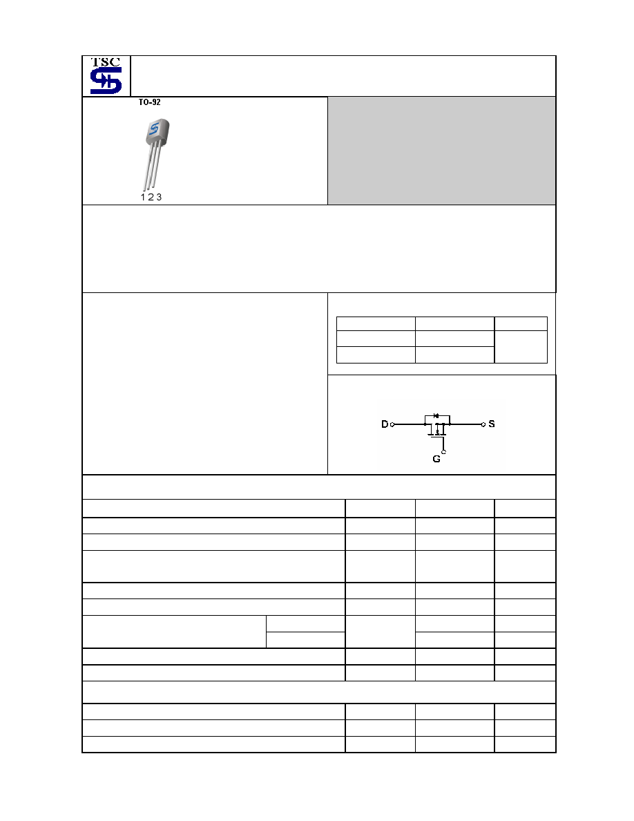
TO-92
Features
High density cell design for low on-resistance
Voltage control small signal switch
Rugged and reliable
High saturation current capability
Provide in TO-92 package
Block Diagram
Absolute Maximum Rating
(Ta = 25
o
C unless otherwise noted)
Parameter Symbol
Limit
Unit
Drain-Source Voltage
V
DS
60 V
Drain-Gate Voltage
V
DGR
60 V
Gate-Source Voltage --- Continuous
--- Pulsed
V
GS
V
GSM
� 20
� 40
V
Continuous Drain Current
I
D
200
mA
Pulsed Drain Current
I
DM
500
mA
Ta = 25
o
C 350
mW
Maximum Power Dissipation
Ta > 25
o
C
P
D
2.8 mW/
o
C
Operating Junction Temperature
T
J
+150
o
C
Operating Junction and Storage Temperature Range
T
J
, T
STG
- 55 to +150
o
C
Thermal Performance
Parameter Symbol
Limit
Unit
Lead Temperature (1/8" from case)
T
L
10 S
Junction to Ambient Thermal Resistance
R
ja
357
o
C/W
Pin assignment:
1. Gate
2. Source
3. Drain

TSM2N7000 2-3
2003/12
rev.
A
Electrical Characteristics
Tj = 25
o
C unless otherwise noted
Parameter Conditions
Symbol
Min Typ Max
Unit
Static
Drain-Source Breakdown Voltage
V
GS
= 0V, I
D
= 10uA
BV
DSS
60 -- -- V
V
GS
= 10V, I
D
= 500mA
R
DS(ON)
-- -- 5.0
Drain-Source On-State Resistance *
V
GS
= 5V, I
D
= 50mA
R
DS(ON)
-- 7.5 --
Drain-Source On-Voltage *
V
GS
= 0V, I
D
= 10uA
V
DS(ON)
-- -- 2.5 V
Gate Threshold Voltage *
V
DS
= V
GS
, I
D
= 1.0mA
V
GS(TH)
0.8 -- 3.0 V
Zero Gate Voltage Drain Current
V
DS
= 48V, V
GS
= 0V
I
DSS
-- -- 1.0
uA
Gate Body Leakage - Forward
V
GS
= 15V, V
DS
= 0V
I
GSS
-- -- -
10
nA
On-State Drain Current
V
DS
5V, V
GS
= 10V
I
D(ON)
60 -- -- mA
Dynamic
Turn-On Rise Time *
t
r
--
10
--
Turn-Off Fall Time *
V
DD
= 15V, R
L
= 30,
I
D
= 500mA,
V
GEN
= 10V, R
G
= 25
t
f
--
10
--
nS
Input Capacitance
C
iss
-- 60 --
Output Capacitance
C
oss
-- 25 --
Reverse Transfer Capacitance
V
DS
= 25V, V
GS
= 0V,
f = 1.0MHz
C
rss
-- 5 --
pF
Source-Drain Diode
Max. Diode Forward Current
I
S
-- --
500
mA
Diode Forward Voltage
I
S
= 200mA, V
GS
= 0V
V
SD
-- 1.3
1.5 V
* Note : pulse test: pulse width <=300uS, duty cycle <=2%