Äîêóìåíòàöèÿ è îïèñàíèÿ www.docs.chipfind.ru
TSM2N7002ED
1-5
2004/12 rev. B
TSM2N7002ED
50V Dual N-Channel Enhancement Mode MOSFET
V
DS
= 50V
R
DS (on)
, Vgs @ 10V, Ids @ 250mA = 3
R
DS (on)
, Vgs @ 5V, Ids @ 50mA = 4
Ordering Information
Part No.
Packing
Package
TSM2N7002EDCU6
T & R (3kpcs/Rell) SOT-363
Features
Dual N-channel in package.
Advanced trench process technology
High density cell design for ultra low on-resistance
High input impedance
High speed switching
No minority carrier storage time
CMOS logic compatible input
No secondary breakdown
Compact and low profile SOT-363 package
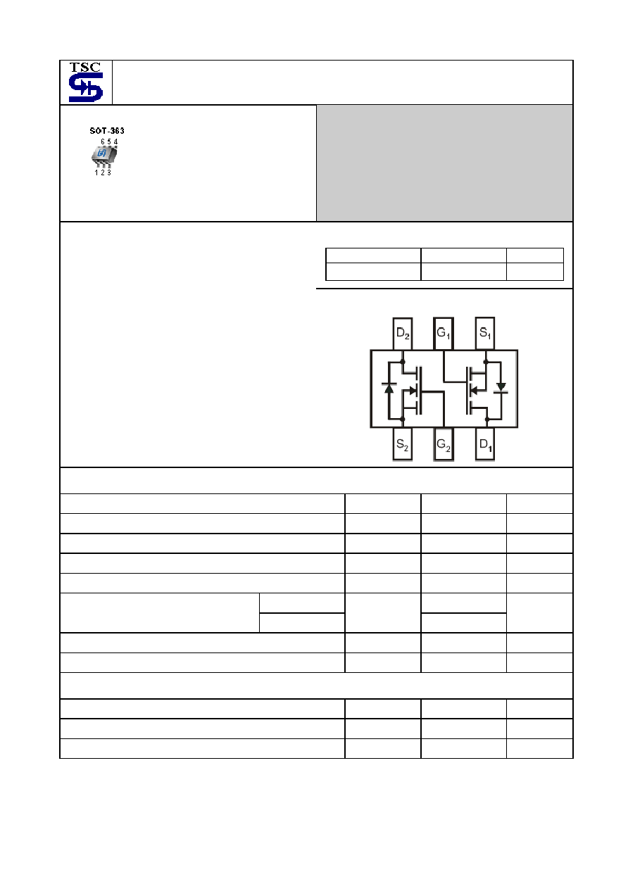
Block Diagram
Absolute Maximum Rating
(Ta = 25
o
C unless otherwise noted)
Parameter Symbol
Limit
Unit
Drain-Source Voltage
V
DS
50 V
Gate-Source Voltage
V
GS
±
20 V
Continuous Drain Current
I
D
250
mA
Pulsed Drain Current
I
DM
1.0 A
Ta = 25
o
C 200
Maximum Power Dissipation
Ta = 75
o
C
P
D
150
mW
Operating Junction Temperature
T
J
+150
o
C
Operating Junction and Storage Temperature Range
T
J
, T
STG
- 55 to +150
o
C
Thermal Performance
Parameter Symbol
Limit
Unit
Lead Temperature (1/8" from case)
T
L
5 S
Junction to Ambient Thermal Resistance (PCB mounted)
R
ja
625
o
C/W
Note: Surface mounted on FR4 board t<=5sec.
Pin assignment:
1. Source (2)
6. Drain (2)
2. Gate (2)
5. Gate (1)
3. Drain (1)
4. Source (1)
TSM2N7002ED
2-5
2004/12 rev. B
Electrical Characteristics (Single Channel)
Tj = 25
o
C unless otherwise noted
Parameter Conditions
Symbol
Min Typ Max
Unit
Static
Drain-Source Breakdown Voltage
V
GS
= 0V, I
D
= 10uA
BV
DSS
50 -- -- V
Drain-Source On-State Resistance
V
GS
= 10V, I
D
= 250mA
R
DS(ON)
-- -- 3
Drain-Source On-State Resistance
V
GS
= 5V, I
D
= 50mA
R
DS(ON)
-- -- 4
Gate Threshold Voltage
V
DS
= V
GS
, I
D
= 250uA
V
GS(TH)
1.0 2.0 2.5 V
Zero Gate Voltage Drain Current
V
DS
= 50V, V
GS
= 0V
I
DSS
-- -- 1.0
uA
Gate Body Leakage
V
GS
= ± 20V, V
DS
= 0V
I
GSS
-- --
±
100
nA
On-State Drain Current
V
DS
7V, V
GS
= 10V
I
D(ON)
500 -- -- mA
Forward Transconductance
V
DS
= 7V, I
D
= 200mA
g
fs
80 -- --
mS
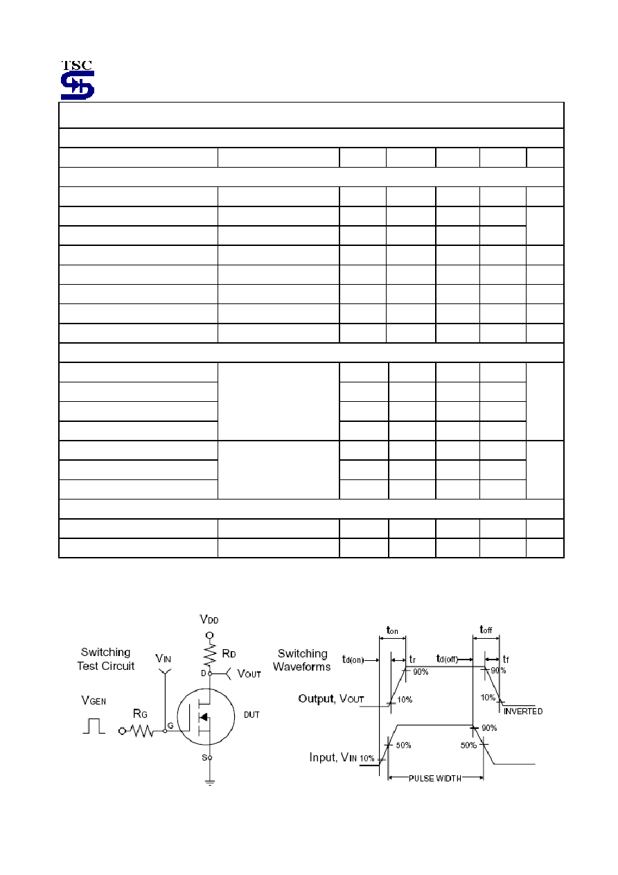
Dynamic *
Turn-On Delay Time
T
D(ON)
-- 7.5 20
Turn-On Rise Time
t
r
-- 6 --
Turn-Off Delay Time
T
D(OFF)
-- 7.5 20
Turn-Off Fall Time
V
DD
= 30V,
I
D
= 100mA, V
GEN
= 10V,
R
G
= 10
t
f
-- 3 --
nS
Input Capacitance
C
iss
-- 19 50
Output Capacitance
C
oss
-- 10 25
Reverse Transfer Capacitance
V
DS
= 25V, V
GS
= 0V,
f = 1.0MHz
C
rss
-- 3 5
pF
Source-Drain Diode
Max. Diode Forward Current
I
S
-- --
115
mA
Diode Forward Voltage
I
S
= 115mA, V
GS
= 0V
V
SD
-- 0.76
1.5 V
Note : pulse test: pulse width <=300uS, duty cycle <=2%
* Guaranteed by design, not subject to production testing.
TSM2N7002ED
3-5
2004/12 rev. B
Typical Characteristics Curve - Single Channel
(Ta = 25
o
C unless otherwise noted)
Gate to source voltage (V)
Drain to source voltage (V)
Drain current (A)
Junction temperature (
o
C)
Gate
s
ourc
e
thre
s
hold v
o
lta
g
e
(
V
)
Ca
p
acitan
ce
(p
F
)
Drain
to
so
u
r
ce resistan
ce
(
)
Drain Current (A)
Drain to source voltage (V)
Drain Current (A)
Junction temperature (
o
C)
Drain
so
u
r
ce b
r
eakd
o
w
n
vo
ltag
e (V)
Output Characteristic
Transfer Characteristics
Rds(on) Variation with Drain Current
Capacitance
Vds breakdown with Temperature
Vgs(th) with Temperature
TSM2N7002ED
4-5
2004/12 rev. B
Typical Characteristics Curve
(Ta = 25
o
C unless otherwise noted)
Drain to source current (A)
Body diode forward voltage (V)
Square wave pulse duration (S)
Drain-source voltage (V)
Total gate charge (nC)
Tra
n
s
c
onduc
ta
nc
e
(S)
Sourc
e
-
dra
i
n Curre
nt (A)
Drain Current (A)
Gate
so
u
r
ce vo
lta
g
e
(
V
)
T
r
an
sien
t th
ermal imp
e
d
a
n
ce r
(
t
)
Transconductance Variation
Normalized Thermal Transient Impedance Curve
Gate Charge
Maximum Safe Operating Area
Body Diode Forward Voltage
TSM2N7002ED
5-5
2004/12 rev. B
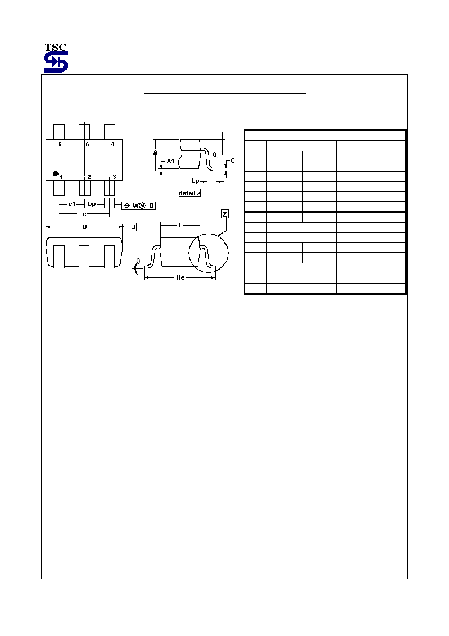
SOT-363 Mechanical Drawing
SOT-363 DIMENSION
MILLIMETERS INCHES
DIM
MIN MAX MIN MAX
A 0.80 1.10 0.031 0.043
A1 -- 0.10 -- 0.004
bp 0.10 0.30 0.004 0.012
C 0.10 0.25 0.004 0.010
D 1.80 2.20 0.071 0.087
E 1.15 1.35 0.045 0.053
e
1.30 (typ)
0.052 (typ)
e1 0.65
(typ)
0.026(typ)
He
2.00 2.20 0.079
0.087
Lp 0.10 0.3 0.004 0.012
Q
0.20 (typ)
0.008 (typ)
W
0.20 (typ)
0.008 (typ)
10
o
(typ) 10
o
(typ)