TSM4835 1-5
2003/12
rev.
A
TSM4835
30V P-Channel Enhancement Mode MOSFET
V
DS
= - 30V
R
DS (on)
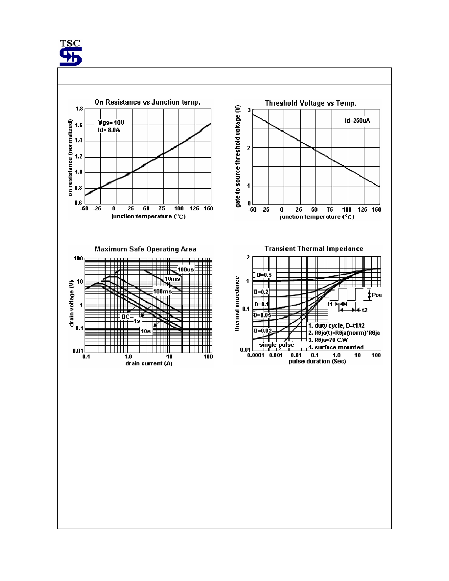
, Vgs @ - 10V, Ids @ - 9.5A =18m
R
DS (on)
, Vgs @ - 4.5V, Ids @ - 7.5A =30m
Features
Advanced trench process technology
High density cell design for ultra low on-resistance
High gate voltage
Ordering Information
Part No.
Packing
Package
TSM4835CS Tape
&
Reel
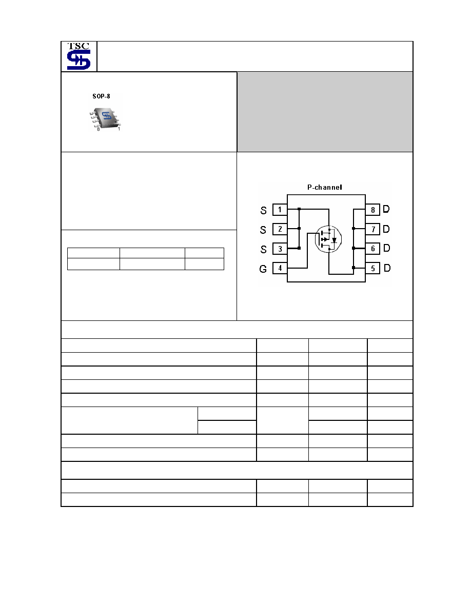
SOP-8
Block Diagram
Absolute Maximum Rating
(Ta = 25
o
C
unless otherwise noted)
Parameter Symbol
Limit
Unit
Drain-Source Voltage
V
DS
-
30 V
Gate-Source Voltage
V
GS
�
25 V
Continuous Drain Current, V
GS
@4.5V.
I
D
- 9.5
A
Pulsed Drain Current, V
GS
@4.5V
I
DM
-
50 A
Ta = 25
o
C 2.5
W
Maximum Power Dissipation
Ta > 25
o
C
P
D
1.6 W
Operating Junction Temperature
T
J
+150
o
C
Operating Junction and Storage Temperature Range
T
J
, T
STG
- 55 to +150
o
C
Thermal Performance
Parameter Symbol
Limit
Unit
Junction to Ambient Thermal Resistance (PCB mounted)
R
ja
50
o
C/W
Note: Surface mounted on FR4 board t<=5sec.
Pin assignment:
1. Source 8. Drain
2. Source 7. Drain
3. Source 6. Drain
4. Gate
5. Drain
TSM4835 2-5
2003/12
rev.
A
Electrical Characteristics
Ta = 25
o
C, unless otherwise noted
Parameter Conditions
Symbol
Min
Typ
Max
Unit
Static
Drain-Source Breakdown Voltage
V
GS
= 0V, I
D
= - 250uA
BV
DSS
-
30 --
-- V
Drain-Source On-State Resistance
V
GS
= - 10V, I
D
= -9.5A
R
DS(ON)
-- 13 18
Drain-Source On-State Resistance
V
GS
= - 4.5V, I
D
= -7.5A
R
DS(ON)
-- 22 30
m
Gate Threshold Voltage
V
DS
= V
GS
, I
D
= - 250uA
V
GS(TH)
-
1 -- -
3 V
Zero Gate Voltage Drain Current
V
DS
= - 30V, V
GS
= 0V
I
DSS
-- -- -
1.0
uA
Gate Body Leakage
V
GS
= � 25V, V
DS
= 0V
I
GSS
-- --
�
100
nA
Forward Transconductance
V
DS
= - 15V, I
D
= - 8A
g
fs
-- 22 -- S
Dynamic
V
DS
= - 15V, I
D
= - 4.6A,
V
GS
= - 5V
-- 23 34
Total Gate Charge
Q
g
-- 54 60
Gate-Source Charge
Q
gs
-- 8.5 --
Gate-Drain Charge
V
DS
= - 15V, I
D
= - 4.6A,
V
GS
= - 10V
Q
gd
--
10.3 --
nC
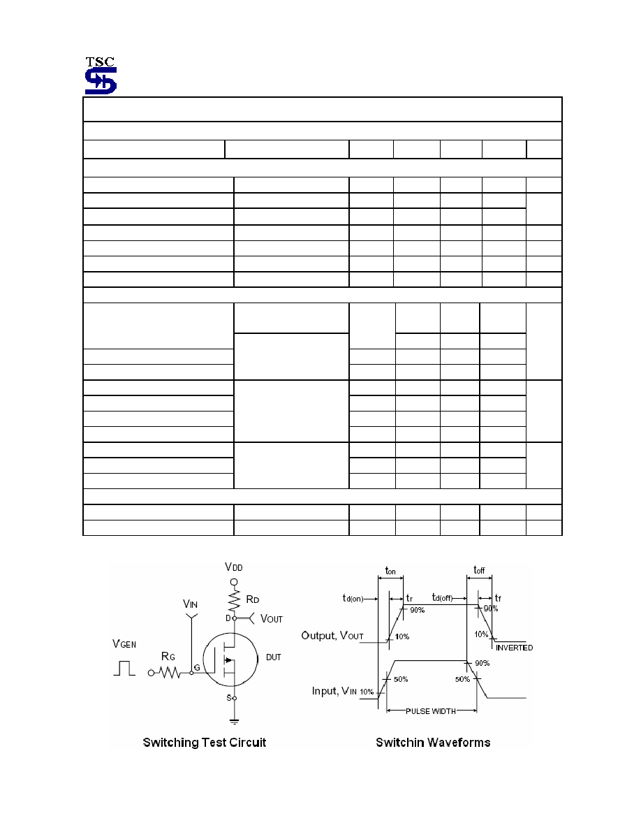
Turn-On Delay Time
t
d(on)
-- 24 30
Turn-On Rise Time
t
r
--
12
30
Turn-Off Delay Time
t
d(off)
-- 78 120
Turn-Off Fall Time
V
DD
= - 15V, R
L
= 15,
I
D
= - 1A, V
GEN
= - 10V,
R
G
= 6
t
f
--
37
80
nS
Input Capacitance
C
iss
--
2520
--
Output Capacitance
C
oss
-- 490 --
Reverse Transfer Capacitance
V
DS
= - 15V, V
GS
= 0V,
f = 1.0MHz
C
rss
-- 330 --
pF
Source-Drain Diode
Max. Diode Forward Current
I
S
-- --
-
2.1
A
Diode Forward Voltage
I
S
= - 2.1A, V
GS
= 0V
V
SD
--
-
0.77
-
1.2
V
Note : pulse test: pulse width <=300uS, duty cycle <=2%
TSM4835 5-5
2003/12
rev.
A
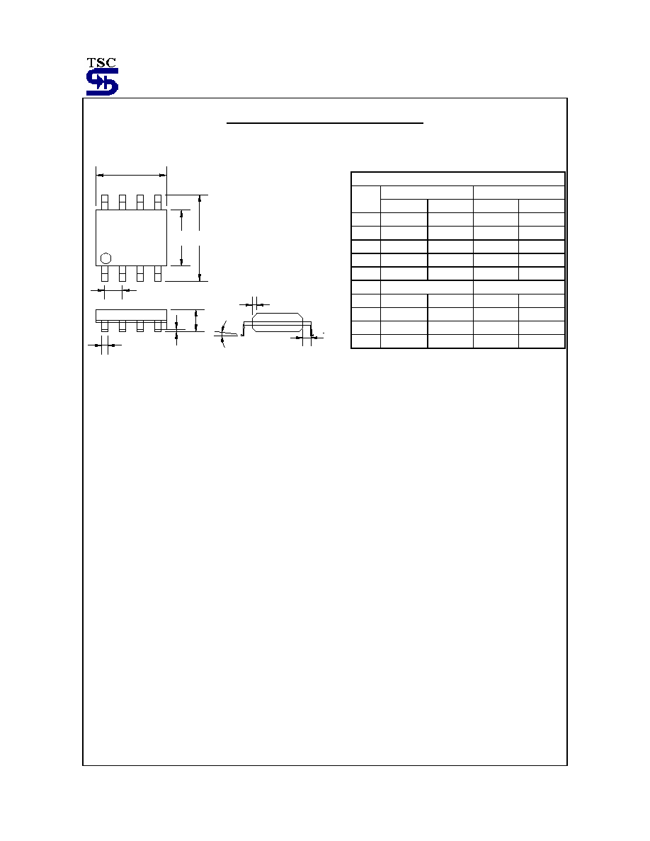
SOP-8 Mechanical Drawing
C
P
B
D
K
G
1
8
A
16
9
R
M
F
SOP-8 DIMENSION
MILLIMETERS INCHES
DIM
MIN MAX MIN MAX
A 4.80 5.00 0.189 0.196
B 3.80 4.00 0.150 0.157
C 1.35 1.75 0.054 0.068
D 0.35 0.49 0.014 0.019
F 0.40 1.25 0.016 0.049
G
1.27 (typ)
0.05 (typ)
K 0.10 0.25 0.004 0.009
M 0
o
7
o
0
o
7
o
P 5.80 6.20 0.229 0.244
R 0.25 0.50 0.010 0.019