CHA2091
Ref. : DSCHA20919340 -06 Dec. 99
1/8
Specifications subject to change without notice
United Monolithic Semiconductors S.A.S.
Route DÈpartementale 128 - B.P.46 - 91401 Orsay Cedex France
Tel. : +33 (0)1 69 33 03 08 - Fax : +33 (0)1 69 33 03 09
36-40GHz Low Noise Amplifier
GaAs Monolithic Microwave IC
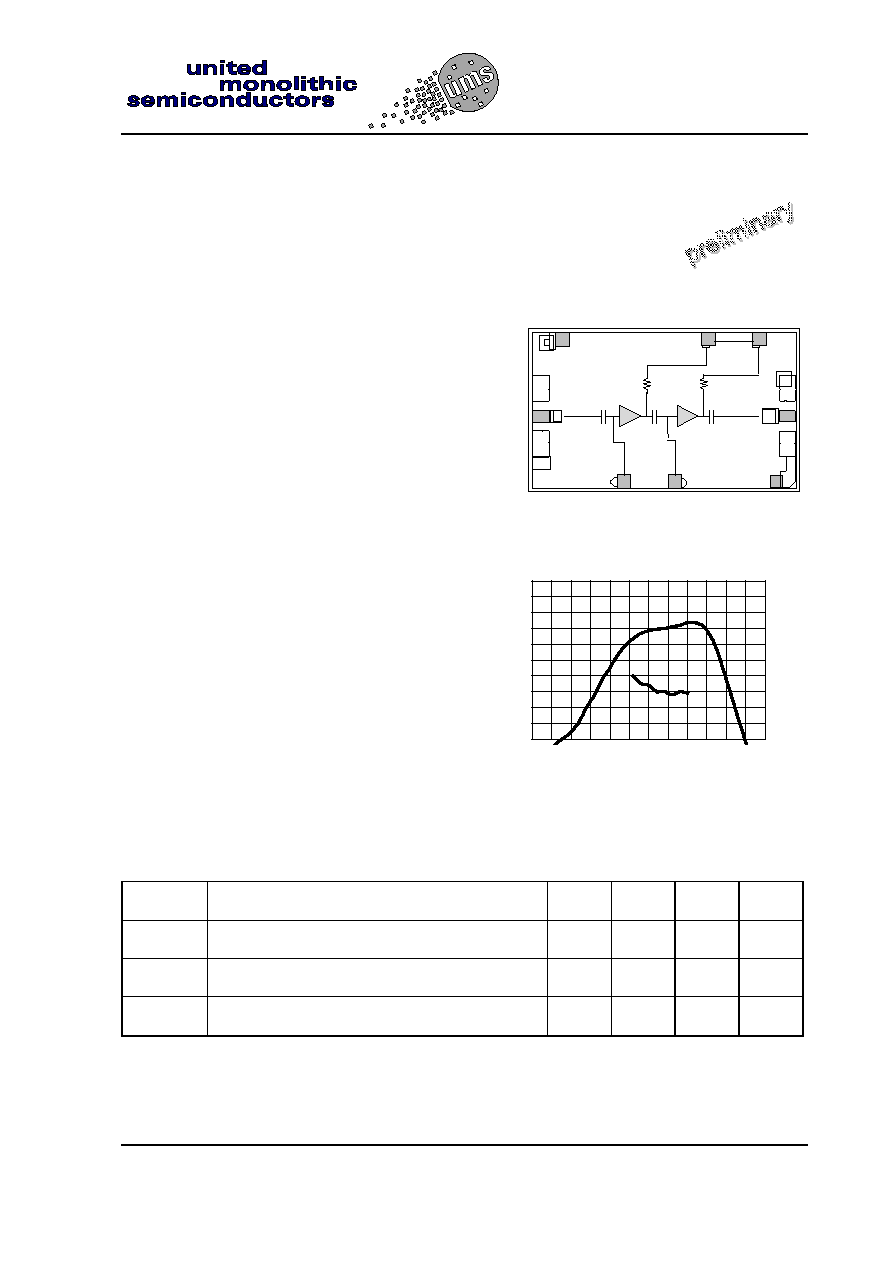
Description
The CHA2091 is a two-stage wide band
monolithic low noise amplifier.
The circuit is manufactured with a standard
HEMT process : 0.25µm gate length, via
holes through the substrate, air bridges
and electron beam gate lithography.
It is supplied in chip form.
Main Features
Broad band performance 36-40GHz
3.0dB noise figure, 36-40GHz
14dB gain,
±
0.5dB gain flatness
Low DC power consumption, 50mA
20dBm 3rd order intercept point
Chip size : 1,67 x 1,03 x 0.1mm
IN
OUT
Vg 1 Vg 2
25
50
Vd
0
2
4
6
8
10
12
14
16
18
20
20
25
30
35
40
45
50
Frequency ( GHz )
Gain ( dB
)
0
1
2
3
4
5
6
7
8
9
10
N
o
i
s
e F
i
gure ( dB
)
On wafer typical measurements.
Main Characteristics
Tamb = +25∞C
Symbol
Parameter
Min
Typ
Max
Unit
NF
Noise figure, 36-40GHz
3.0
4.0
dB
G
Gain
12
14
dB
G
Gain flatness
±
0.5
±
1.0
dB
ESD Protections : Electrostatic discharge sensitive device observe handling precautions !
CHA2091
36-40GHz Low Noise Amplifier
Ref. : DSCHA20919340 -06 Dec. 99
2/8
Specifications subject to change without notice
Route DÈpartementale 128 , B.P.46 - 91401 ORSAY Cedex - FRANCE
Tel.: +33 (0)1 69 33 03 08 - Fax : +33 (0)1 69 33 03 09
Electrical Characteristics
Tamb = +25∞C,
Bias Conditions:Vd = +4V Id=45mA
Symbol
Parameter
Min
Typ
Max
Unit
Fop
Operating frequency range
36
40
Ghz
G
Gain (1)
12
14
dB
G
Gain flatness (1)
±
0.5
±
1.0
dB
NF
Noise figure (1)
3.0
4.0
dB
VSWRin
Input VSWR (1)
3.0:1
VSWRout Ouput VSWR (1)
3.0:1
IP3
3rd order intercept point
20
dBm
P1dB
Output power at 1dB gain compression
12
dBm
Id
Drain bias current
50
mA
(1) These values are representative of on-wafer measurements that are made without
bonding wires at the RF ports.When the chip is attached with typical 0.15nH input and
output bonding wires, the indicated parameters should be improved.
Absolute Maximum Ratings
(1)
Tamb = +25∞C
Symbol
Parameter
Values
Unit
Vd
Drain bias voltage
4.0
V
Pin
Maximum peak input power overdrive (2)
+15
dBm
Top
Operating temperature range
-40 to +85
∞C
Tstg
Storage temperature range
-55 to +125
∞C
(1) Operation of this device above anyone of these paramaters may cause permanent damage.
(2) Duration < 1s.
36-40GHz Low Noise Amplifier
CHA2091
Ref. : DSCHA20919340 -06 Dec. 99
3/8
Specifications subject to change without notice
Route DÈpartementale 128 , B.P.46 - 91401 ORSAY Cedex - FRANCE
Tel.: +33 (0)1 69 33 03 08 - Fax : +33 (0)1 69 33 03 09
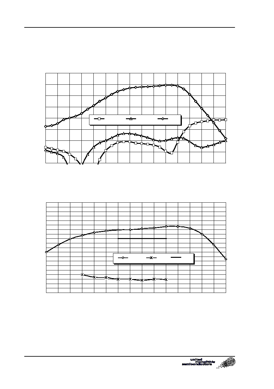
Typical Results
Chip Typical Response ( On wafer Sij ) :
Tamb = +25∞C
Bias conditions: Vd = +4V, Id=45mA
Freq
GHz
MS11
dB
PS11
∞
MS12
dB
PS12
∞
MS21
dB
PS21
∞
MS22
dB
PS22
∞
10
-6
170.2
-57.3
-141
-12.4
11.3
-5.68
177.7
12
-7.1
156.5
-54.1
-157
-9.98
-12.7
-6.93
152.9
14
-8.42
145.2
-50.3
173.7
-8.72
-32.7
-8.54
131.2
16
-10
137
-48.1
158
-6.92
-51.3
-9.44
113
18
-11.5
132.1
-49.6
138.4
-5.05
-71.3
-11.3
93
20
-13
129
-47.8
120.7
-3.74
-93.7
-14.2
81.8
21
-13.6
127.7
-48.2
107
-3.31
-101
-15.1
80.4
22
-14.2
126.6
-49.1
114.5
-2.37
-107
-15.8
75.6
23
-14.8
122.7
-50.1
130.8
-0.72
-117
-17.5
61.4
24
-16.1
116.3
-45.5
130.2
0.08
-130
-23.2
51.5
25
-18.2
111
-42.9
121.1
0.86
-138
-32.6
132.7
26
-21.8
108.1
-42.2
109.7
2.11
-146
-21.7
167.7
27
-30
127.3
-40.8
107
3.95
-156
-16.2
165.6
28
-26.2
-140
-39.6
104.3
5.61
-169
-12.9
151.8
29
-18.5
-136
-36.8
93
7.52
176
-11
140.8
30
-14.5
-146
-34.8
85
8.99
157.9
-9.98
128.3
31
-12.3
-159
-32.5
68.7
10.58
139.4
-8.78
121.3
32
-10.9
-173
-31.8
48.3
11.88
117.3
-7.48
109.9
33
-10.5
174.9
-30.8
28.7
12.69
94.8
-6.88
95.3
34
-10.5
165.2
-29.8
7.3
13.36
72.8
-6.94
82.8
35
-11.1
156.1
-29.6
-15.2
13.72
50.2
-7.25
70.8
36
-11.3
150.5
-29.5
-33.9
13.93
28.2
-7.94
60.9
37
-11.6
144
-30.1
-55.6
13.99
6.7
-8.73
52.2
38
-12
133
-29.6
-69.8
14.2
-14.5
-9.57
47.1
39
-12.9
115.4
-28.7
-85.8
14.39
-37.1
-10.2
43.7
40
-14.7
87.2
-29
-120
14.65
-61.2
-9.88
40.4
41
-15.5
25.3
-28.1
-144
14.71
-88.7
-9.19
30.1
42
-10.7
-42.3
-27.8
-176
14.34
-121
-8.66
10.8
43
-6.09
-86.6
-28.3
146.7
12.98
-154
-8.99
-16.9
44
-3.4
-119
-30.4
111.9
10.59
174.3
-10.5
-50
45
-2.22
-143
-32.9
90
7.53
147.6
-12.2
-83.8
46
-1.59
-160
-35.2
62.9
4.31
125.2
-13
-119
47
-1.15
-175
-35.3
39
1.21
105.5
-12.5
-149
48
-0.84
173.2
-43.5
-26.6
-2.06
88.2
-11.8
-174
49
-0.85
163.7
-39.4
27.3
-5.61
72.6
-10.8
169
50
-0.67
154.7
-36.9
31.8
-9.07
58.2
-10.1
156.4
CHA2091
36-40GHz Low Noise Amplifier
Ref. : DSCHA20919340 -06 Dec. 99
4/8
Specifications subject to change without notice
Route DÈpartementale 128 , B.P.46 - 91401 ORSAY Cedex - FRANCE
Tel.: +33 (0)1 69 33 03 08 - Fax : +33 (0)1 69 33 03 09
Typical Results
Chip Typical Response ( On wafer Sij ) :
Tamb = +25∞C
Vd = +4V Id=45mA
-20
-15
-10
-5
0
5
10
15
20
20
22
24
26
28
30
32
34
36
38
40
42
44
46
48
50
Frequency ( GHz )
G
a
in, RLoss ( dB )
DBS11
DBS22
Gain
Typical Gain and Matching measurements on wafer.
0
1
2
3
4
5
6
7
8
9
10
11
12
13
14
15
16
17
18
19
20
30
31
32
33
34
35
36
37
38
39
40
41
42
43
44
45
Frequency ( GHz )
G
a
in, NF (
dB )
Gain
NF
Gab
Typical Gain and Noise Figure measurements on wafer.
36-40GHz Low Noise Amplifier
CHA2091
Ref. : DSCHA20919340 -06 Dec. 99
5/8
Specifications subject to change without notice
Route DÈpartementale 128 , B.P.46 - 91401 ORSAY Cedex - FRANCE
Tel.: +33 (0)1 69 33 03 08 - Fax : +33 (0)1 69 33 03 09
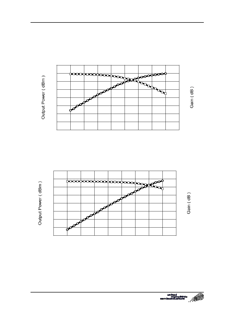
Typical Results
Tamb = +25∞C
Vd = 4V ; Id = 45mA
Freq = 37GHz
0
2
4
6
8
10
12
14
16
-12
-10
-8
-6
-4
-2
0
2
4
6
Input Power ( dBm )
0
2
4
6
8
10
12
14
16
Freq = 39.5GHz
0
2
4
6
8
10
12
14
16
-14
-12
-10
-8
-6
-4
-2
0
2
4
Input Power ( dBm )
0
2
4
6
8
10
12
14
16
Typical Output Power and Gain measurements in test jig
(included losses of the jig)