
CHA2092b
Ref. : DSCHA20921233 21-August-01
1/6
Specifications subject to change without notice
United Monolithic Semiconductors S.A.S.
Route Dťpartementale 128 - B.P.46 - 91401 Orsay Cedex France
Tel. : +33 (0)1 69 33 03 08 - Fax : +33 (0)1 69 33 03 09
18-32GHz Low Noise Amplifier
GaAs Monolithic Microwave IC
Description
The CHA2092 is a high gain broadband three-
stage monolithic low noise amplifier. It is
designed for a wide range of applications, from
military to commercial communication
systems. The backside of the chip is both RF
and DC ground. This helps simplify the assembly
process. Self biasing technique is implemented
on chip to ease the circuit biasing.
The circuit is manufactured with a P-HEMT
process, 0.25Ķm gate length, via holes through
the substrate, air bridges and electron beam
gate lithography.
It is available in chip form.
Main Features
Broadband performances : 18-32GHz
2.5dB Noise Figure
10dBm output power ( -1dB gain comp. )
22dB
Ī
1.0dB gain
Low DC power consumption, 60mA @ 3.5V
Chip size : 1.67 X 0.97 X 0.10 mm
Vgs1
Vgs2,3
Vds
IN
OUT
8831
0
5
10
15
20
25
30
15 17 19 21 23 25 27 29 31 33 35
Frequency (GHz)
Gain & NF ( dB )
Main Characteristics
Tamb. = 25įC
Symbol Parameter Min
Typ
Max
Unit
Fop
Operating frequency range
18
32
GHz
G
Small signal gain
17
22
dB
NF
Noise figure (20-32GHz)
2.5
3.5
dB
P1dB
Output power at 1dB gain compression
8
10
dBm
Id Bias
current
60 100 mA
ESD Protection : Electrostatic discharge sensitive device. Observe handling precautions !

CHA2092b
18-32GHz Low Noise Amplifier
Ref. : DSCHA20921233 21-August-01
2/6
Specifications subject to change without notice
Route Dťpartementale 128 , B.P.46 - 91401 ORSAY Cedex - FRANCE
Tel.: +33 (0)1 69 33 03 08 - Fax : +33 (0)1 69 33 03 09
Electrical Characteristics
Tamb = +25įC, Vds = 3.5V; Ids=60mA
Symbol
Parameter
Min Typ Max
Min Typ Max Unit
Fop
Operating frequency range (1)
20
28
18
32
GHz
G
Small signal gain (1)
18
22
17
22
dB
G
Small signal gain flatness (1)
Ī
1.5
Ī
2.5
dB
Gsb
Gain flatness over 40MHz
0.5
0.5
dBpp
Is
Reverse isolation (1)
25
30
25
30
dB
P1dB
Output power at 1dB gain compression (3)
8
10
8
10
dBm
VSWRin Input VSWR (1)
2.5:1 3.0:1
2.5:1 3.5:1
VSWRout Output VSWR (1)
2.5:1 3.0:1
2.5:1 3.5:1
NF
18-20GHz
Noise figure (2) 20-28GHz
28-32GHz
2.5
3.5
2.5
2.5
2.5
4
3.5
3.5
dB
Vd DC
Voltage
Vd
Vgs1,Vgs2&3
3.5
-0.5
4.5
3.5
-0.5
4.5
V
V
Id
Bias current (2)
60
100
60
100
mA
(1)These values are representative of on-wafer measurements that are made without bonding
wires at the RF ports.
(2) 60 mA is the typical bias current used for on wafer measurements, with Vgs1 and Vgs2&3
connected together. For optimum noise figure, the bias current could be reduced down to
50 mA, adjusting the Vgs1 voltage.
(3) Ids=90mA
Absolute Maximum Ratings
Tamb. = 25įC (1)
Symbol Parameter
Values
Unit
Vd
Drain bias voltage
5.0
V
Id
Drain bias current
120
mA
Vg
Gate bias voltage
-2.0 to +0.4
V
Pin
Maximum peak input power overdrive (2)
+15
dBm
Ta
Operating temperature range
-40 to +85
įC
Tstg
Storage temperature range
-55 to +155
įC
(1) Operation of this device above anyone of these parameters may cause permanent damage.
(2) Duration < 1s.
18-32GHz Low Noise Amplifier
CHA2092b
Ref. : DSCHA20921233 21-August-01
3/6
Specifications subject to change without notice
Route Dťpartementale 128 , B.P.46 - 91401 ORSAY Cedex - FRANCE
Tel.: +33 (0)1 69 33 03 08 - Fax : +33 (0)1 69 33 03 09
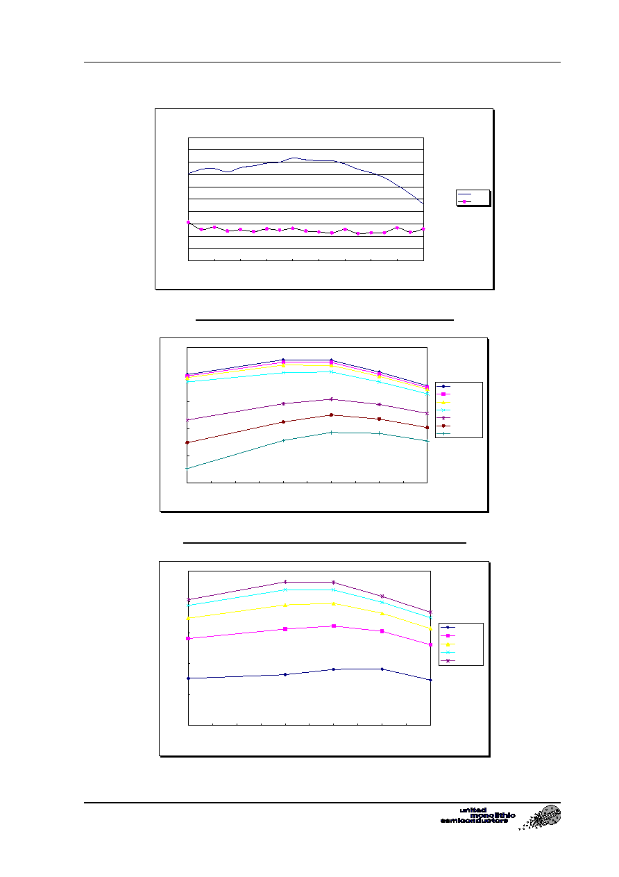
Typical Results
Tamb=25įC
15,00
16,00
17,00
18,00
19,00
20,00
21,00
22,00
23,00
24,00
25,00
17,00
19,00
21,00
23,00
25,00
27,00
29,00
31,00
33,00
35,00
Frequency (GHz)
Gain
(
d
B)
0,00
1,00
2,00
3,00
4,00
5,00
6,00
7,00
8,00
9,00
10,00
NF
(
d
B)
DBS21
NF
Gain and NF vs Frequency (Vdd=3.5V; Ids=60mA)
0
5
10
15
20
25
20
21
22
23
24
25
26
27
28
29
30
Frequency (GHz)
G
a
in
(
d
B)
Vgs1=-0.36V
Vgs1=-0.5V
Vgs1=-0.6V
Vgs1=-0,7V
Vgs1=-0,8V
Vgs1=-0,9V
Vgs1=-1V
Gain vs Frequency and Vgs1 (Vdd=3.5V; Vgs23=-0.3V)
0
5
10
15
20
25
20
21
22
23
24
25
26
27
28
29
30
Frequency (GHz)
G
a
in
(
d
B
)
Vgs=-0,7V
Vgs=-0.6V
Vgs=-0.5V
Vgs=-0.4V
Vgs=-0.3V
CHA2092b
18-32GHz Low Noise Amplifier
Ref. : DSCHA20921233 21-August-01
4/6
Specifications subject to change without notice
Route Dťpartementale 128 , B.P.46 - 91401 ORSAY Cedex - FRANCE
Tel.: +33 (0)1 69 33 03 08 - Fax : +33 (0)1 69 33 03 09
Gain vs Frequency and Vgs123 (Vdd=3.5V)
-16
-14
-12
-10
-8
-6
-4
-2
0
20,00
21,00
22,00
23,00
24,00
25,00
26,00
27,00
28,00
29,00
30,00
Frequency (GHz)
d
B
S11 (
d
B
)
-0,36
-0,50
-0,60
-0,70
-0,80
-0,90
-1,00
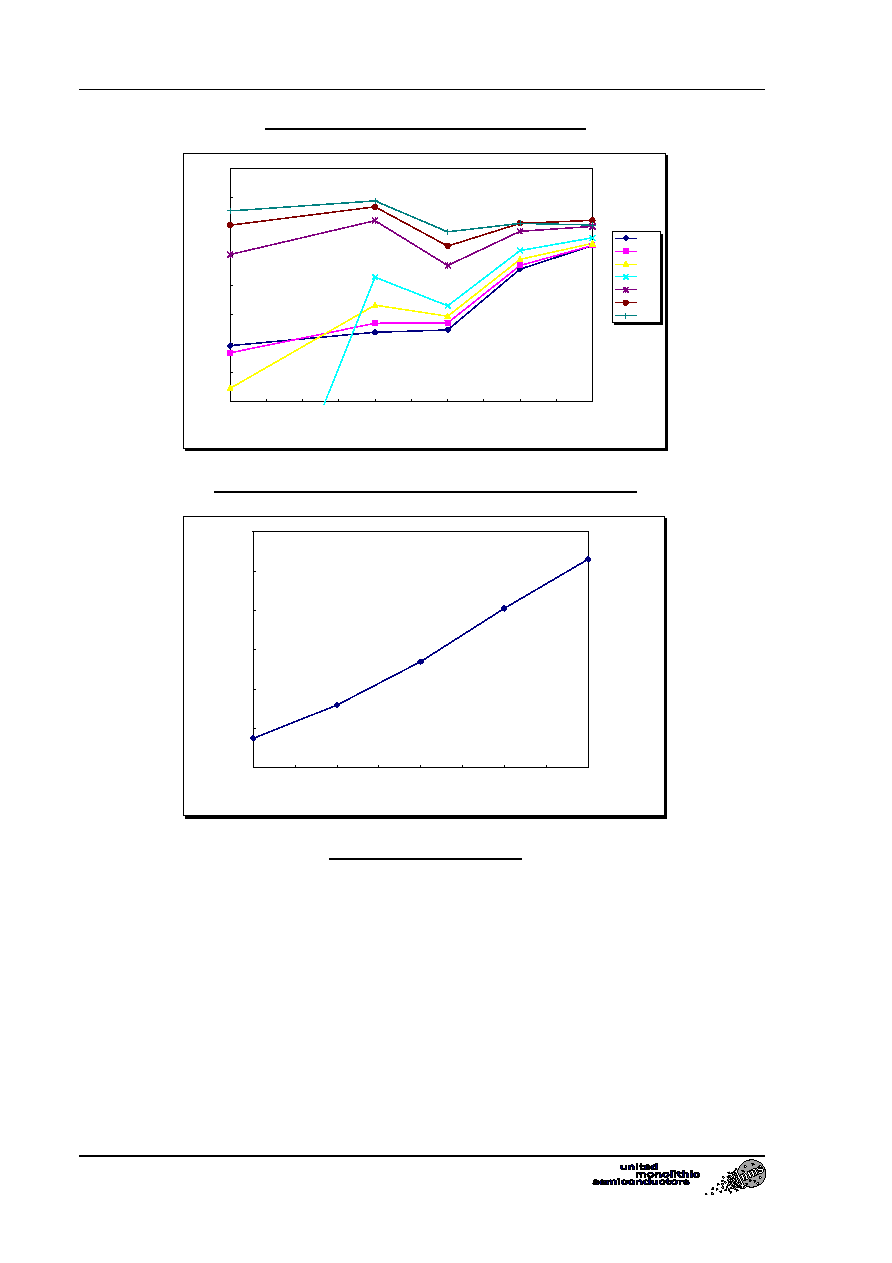
dBS11 vs Frequency and Vgs1 (Vdd=3.5V; Vgs23=-0.3V)
-
20,0
40,0
60,0
80,0
100,0
120,0
-0,70
-0,65
-0,60
-0,55
-0,50
-0,45
-0,40
-0,35
-0,30
Vgs123 (V)
Id
s
(mA
)
Ids vs Vgs123 (Vdd=3.5V)

18-32GHz Low Noise Amplifier
CHA2092b
Ref. : DSCHA20921233 21-August-01
5/6
Specifications subject to change without notice
Route Dťpartementale 128 , B.P.46 - 91401 ORSAY Cedex - FRANCE
Tel.: +33 (0)1 69 33 03 08 - Fax : +33 (0)1 69 33 03 09
Chip Assembly and Mechanical Data
IN
OUT
100pF
100pF
To Vdd DC Drain supply feed
To Vgs DC Gate supply feed.
100pF
To Vgs DC Gate supply feed
to ajust NF.
8831
Note : Supply feed should be capacitively bypassed.
1670 +/- 10
1005
385
325
970 +/- 10
385
920
8831
Bonding pad positions.
( Chip thickness : 100Ķm. All dimensions are in micrometers )