 | –≠–ª–µ–∫—Ç—Ä–æ–Ω–Ω—ã–π –∫–æ–º–ø–æ–Ω–µ–Ω—Ç: CHA2266 | –°–∫–∞—á–∞—Ç—å:  PDF PDF  ZIP ZIP |
CHA2266
Ref. : DSCHA22662242 - 30-Aug.-02
1/7
Specifications subject to change without notice
United Monolithic Semiconductors S.A.S.
Route DÈpartementale 128 - B.P.46 - 91401 Orsay Cedex France
Tel. : +33 (0)1 69 33 03 08 - Fax : +33 (0)1 69 33 03 09
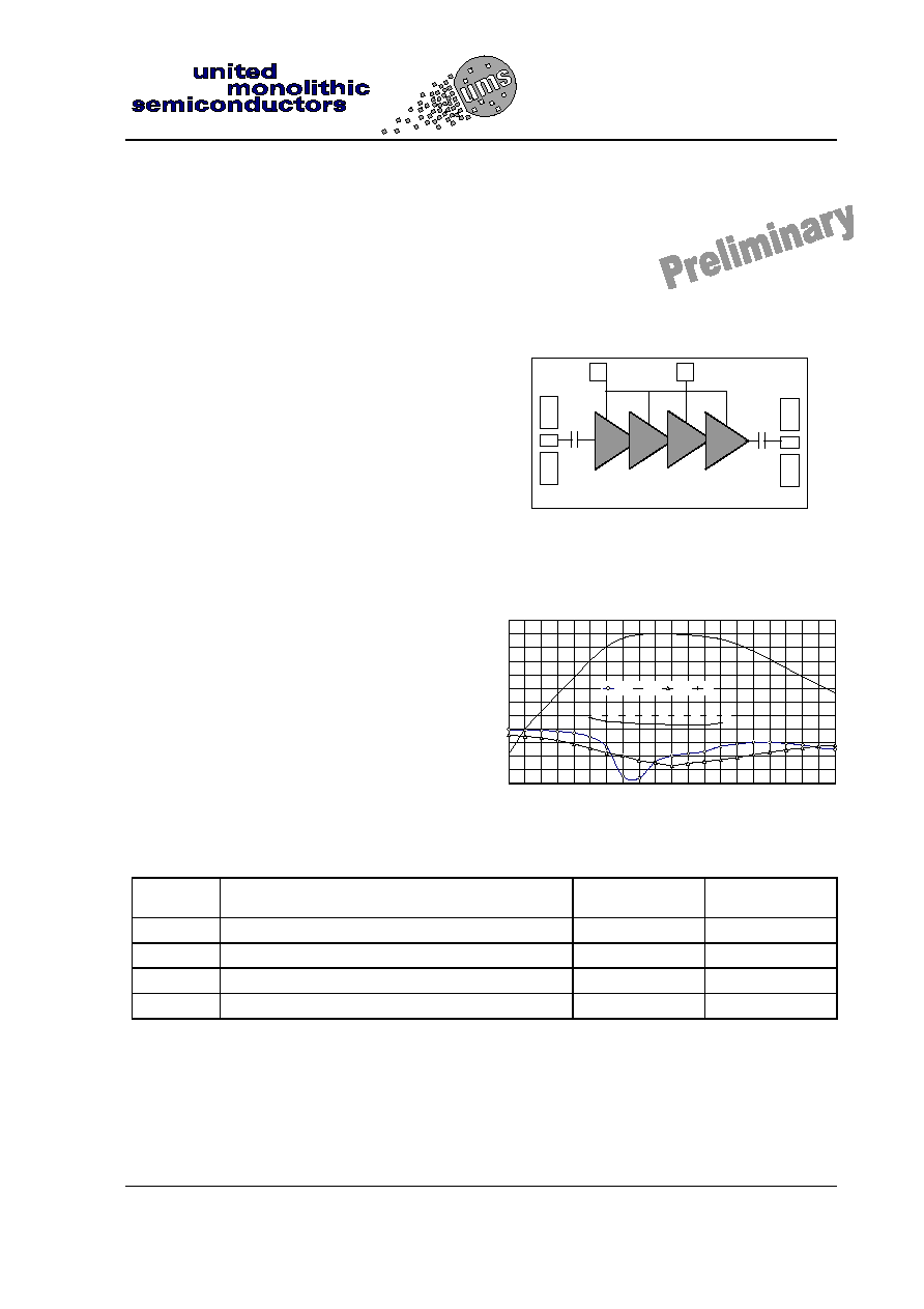
12.5-17GHz Low-Noise Driver Amplifier
GaAs Monolithic Microwave IC
Description
The CHA2266 is a self biased, low-noise high
gain driver amplifier. It is designed mainly for
VSAT applications in Ku-band. The backside of
the chip is both RF and DC grounded. This
helps to simplify the assembly process.
The circuit is manufactured on a standard GaAs
PHEMT process, with via holes through the
substrate, air bridges and electron beam gate
lithography.
Main Features
∑
Broad band performance 12.5≠17GHz
∑
2.5dB noise figure
∑
34dB gain, +/- 0.5dB gain flatness
∑
Low DC power consumption:130mA
∑
Saturated output power : 16dBm
∑
Chip size 2.32 x 1.02 x 0.1mm
Typical on wafer measurements
Absolute maximum Ratings (1)
Symbol Parameter
(1)
Values
Unit
Vd
Drain bias voltage
4.3
V
Pin
Maximum continious input power overdrive
-15
dBm
Top
Operating temperature range
-40 to +85
∞C
Tstg
Storage temperature
-55 to +125
∞C
(1) Operation of this device above any of these parameters may cause permanent damage.
ESD Protection : Electrostatic discharge sensitive device. Observe handling precautions !
VD 1
VD 2
IN
OUT
Typical CHA2266
( Vds = 4V, Ids = 130mA )
2.2
1.5
1.5
1.6
1.9
2.0
2.5
2.9
4.1
-20
-15
-10
-5
0
5
10
15
20
25
30
35
40
5
6
7
8
9
10
11
12
13
14
15
16
17
18
19
20
21
22
23
24
25
Frequency / GHz
G
a
i
n
&
R
e
tur
n
l
o
s
s
/ dB
MS11
MS21
MS22
NF
CHA2266
12.5-17GHz Driver Amplifier
Ref. : DSCHA22662242 - 30-Aug.-02
2/7
Specifications subject to change without notice
Route DÈpartementale 128 , B.P.46 - 91401 ORSAY Cedex - FRANCE
Tel.: +33 (0)1 69 33 03 08 - Fax : +33 (0)1 69 33 03 09
Electrical Characteristicts
Tamb = +25∞C, Vdd = 4V
Symbol Parameter Min
Typ
Max
Unit
Fop
Operating frequency range
12.5
17
GHz
G
Small signal gain
34
dB
G
Small signal gain flatness
±
0.5
dB
NF Noise
Figure
2.5 3.0 dB
RLin
Input return loss
-10
dB
RLout
Output return loss
-10
dB
P1dB
Output power at 1 dB gain compression
14
15
dBm
Pin
Maximum peak input overdrive (1)
15
dBm
Vdd
Drain bias voltage
4
V
Id small
signal
Drain bias current
130
mA
(1) Duration < 1s
Typical Results
Typical Chip Response ( On wafer S-parameter*)
*
Return loss improves with bondings
.
Typical CHA2266
( Vds = 4V, Ids = 130mA )
4.1
2.9
2.5
2.0
1.9
1.6
1.5
1.5
2.2
-20
-15
-10
-5
0
5
10
15
20
25
30
35
40
5
6
7
8
9
10
11
12
13
14
15
16
17
18
19
20
21
22
23
24
25
Frequency / GHz
G
a
in
& Re
tu
rn
lo
s
s
/ d
B
MS11
MS21
MS22
NF
CHA2266
12.5-16 GHz Driver Amplifier
Ref. : DSCHA22662242 - 30-Aug.-02
3/7
Specifications subject to change without notice
Route DÈpartementale 128 , B.P.46 - 91401 ORSAY Cedex - FRANCE
Tel.: +33 (0)1 69 33 03 08 - Fax : +33 (0)1 69 33 03 09
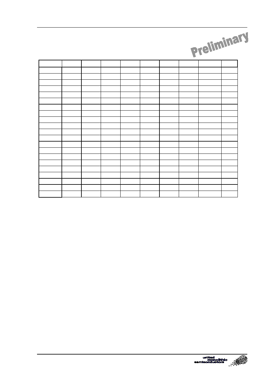
Typical On Wafer Scattering Parameters:
Tamb = +25∞C, Bias Conditions: Vd = 4V, Id = 130mA
Freq/GHz MS11 PS11 MS12 PS12 MS21 PS21 MS22 PS22 NF
5.00 -0.19 -60.43 -80.46 -28.08 -9.27 55.33 -2.21 -70.44
6.00 -0.30 -74.26 -78.78 -70.24 -0.12 -24.96 -2.68 -82.41
7.00 -0.46 -89.33 -75.88 2.69 6.56 -88.05 -3.27 -95.03
8.00 -0.80
-106.32
-72.20
32.17
12.83
-142.23
-4.19
-107.99
9.00
-1.44 -125.75 -73.72 -51.84 19.02 165.74 -5.51 -118.06
10.00 -2.86
-151.22
-66.33
-115.35
25.20
108.42
-7.08 -126.35
4.06
11.00 -6.63 177.56 -70.35 -76.43 30.42 42.05 -8.70 -131.49 2.88
12.00 -17.39
153.85
-66.55
-128.54
33.53 -28.39 -9.87 -134.03 2.46
13.00 -18.06 -84.40 -65.32 168.52 34.77 -94.85 -11.53 -135.84 2.01
14.00 -12.00
-98.21 -59.86
-136.83
35.15
-154.68
-12.46 -131.75 1.92
15.00 -9.86 -113.78 -76.73 168.29 35.05 149.44 -13.41 -127.10 1.60
16.00 -9.01 -121.29 -56.32 80.85 34.64 97.72 -12.58 -114.59 1.55
17.00 -8.27
-129.83
-57.21
-170.04
34.05 46.71
-11.91
-113.66
1.46
18.00 -6.40 -139.02 -62.54 -89.64 33.15 -4.88 -11.24 -113.55 2.24
19.00 -5.55 -156.24 -65.06 53.72 31.28 -55.40 -10.37 -116.41
20.00 -4.88 -174.36 -67.73 -90.69 28.65 -101.56
-9.43 -117.46
21.00 -4.83 166.53 -55.41 154.09 25.68 -143.31
-8.53 -120.11
22.00 -5.31 149.22 -53.79 91.59 22.47 -179.42
-7.66 -125.61
23.00 -5.85 132.80 -52.72 -168.14
19.33 148.56 -7.00 -131.61
24.00 -6.91 118.54 -50.50 80.81 16.33 119.70 -6.35 -137.67
25.00 -7.45
103.68
-71.86
-7.37 13.42 93.05 -6.02 -145.44
CHA2266
12.5-17GHz Driver Amplifier
Ref. : DSCHA22662242 - 30-Aug.-02
4/7
Specifications subject to change without notice
Route DÈpartementale 128 , B.P.46 - 91401 ORSAY Cedex - FRANCE
Tel.: +33 (0)1 69 33 03 08 - Fax : +33 (0)1 69 33 03 09
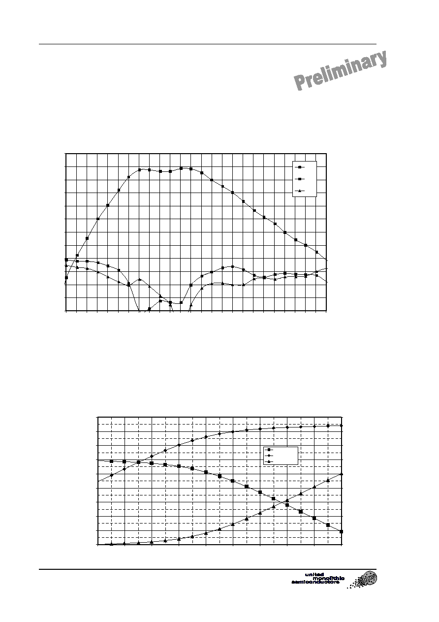
Typical Test-Jig Results
S- Parameters @ small signal
Tamb 25 ∞C, Vd = 4V, Id = 130mA
Pin vs. Pout for 14, 15 and 16GHz
Tamb = 25∞C,Vd =4 V, IDmax 170mA
Gain / Pout @ 14GHz
22
24
26
28
30
32
34
36
38
40
-25
-23
-21
-19
-17
-15
-13
-11
-9
-7
Pin / dBm
G
a
in
/ d
B
0
2
4
6
8
10
12
14
16
18
Gain
Pout
Compression
CHA2266
-20
-15
-10
-5
0
5
10
15
20
25
30
35
40
5
6
7
8
9
10
11
12
13
14
15
16
17
18
19
20
21
22
23
24
25
26
27
28
29
30
Frequency
G
a
in, Re
tur
n
los
s
/ dB
S11
S21
S22

CHA2266
12.5-16 GHz Driver Amplifier
Ref. : DSCHA22662242 - 30-Aug.-02
5/7
Specifications subject to change without notice
Route DÈpartementale 128 , B.P.46 - 91401 ORSAY Cedex - FRANCE
Tel.: +33 (0)1 69 33 03 08 - Fax : +33 (0)1 69 33 03 09
Gain / Pout @ 15GHz
22
24
26
28
30
32
34
36
38
40
-25
-23
-21
-19
-17
-15
-13
-11
-9
-7
Pin / dBm
Gain
/ d
B
0
2
4
6
8
10
12
14
16
18
P
out /
dBm
Gain
Pout
Compression
Gain / Pout @ 16GHz
22
24
26
28
30
32
34
36
38
40
-25
-23
-21
-19
-17
-15
-13
-11
-9
-7
Pin / dBm
G
a
in / dB
0
2
4
6
8
10
12
14
16
18
P
out / dBm
Gain
Pout
Compression