ChipFind - документация

Электронный компонент: CHA2394-99F/00

Скачать:  PDF   ZIP
CHA2394
Ref. : DSCHA23942240 -28-Aug.-02
1/8
Specifications subject to change without notice
United Monolithic Semiconductors S.A.S.
Route Dpartementale 128 - B.P.46 - 91401 Orsay Cedex France
Tel. : +33 (0)1 69 33 03 08 - Fax : +33 (0)1 69 33 03 09
36-40GHz Very Low Noise High Gain Amplifier
GaAs Monolithic Microwave IC
Description
The CHA2394 is a three-stage monolithic
low noise amplifier. It is designed for a wide
range of applications, from military to
commercial communication systems.

The circuit is manufactured with a HEMT
process : 0.25m gate length, via holes
through the substrate, air bridges and
electron beam gate lithography.
It is available in chip form.

Main Features
Broadband performances : 36-40GHz
2.5dB Noise Figure
21dB gain
1.5dB gain flatness
Low DC power consumption, 60mA @
3.5V
Chip size : 1.72 X 1.08 X 0.10 mm


Vgs1&2
Vgs3
Vds
IN
OUT
Vds


Typical on wafer measurements :
Main Characteristics
Tamb. = 25C
Symbol Parameter Min
Typ
Max
Unit
Fop
Operating frequency range
36
40
GHz
G
Small signal gain
18
21
dB
P1dB
Output power at 1dB gain compression
8
12
dBm
NF Noise
figure
2.5 3.0 dB

ESD Protection : Electrostatic discharge sensitive device. Observe handling precautions !
10
12
14
16
18
20
22
30 31 32 33 34 35 36 37 38 39 40
Frequency (GHz)
Ga
i
n
(d
B
)
1
1,5
2
2,5
3
3,5
4
NF
(
d
B
)
CHA2394
36-40GHz Very Low Noise Amplifier
Ref. : DSCHA23942240 -28-Aug.-02
2/8
Specifications subject to change without notice
Route Dpartementale 128 , B.P.46 - 91401 ORSAY Cedex - FRANCE
Tel.: +33 (0)1 69 33 03 08 - Fax : +33 (0)1 69 33 03 09
Electrical Characteristics
Tamb = +25C, Vd1,2,3 = 3.5V
Symbol Parameter Min
Typ
Max
Unit
Fop
Operating frequency range (1)
36
40
GHz
G
Small signal gain (1)
18
21
dB
G
Small signal gain flatness (1)
1.5
dB
Gsb
Gain flatness over 40MHz ( within -30 ; +75C )
0.5
dBpp
Is
Reverse isolation (1)
25
30
dB
P1dB
Output power at 1dB gain compression
5
8
dBm
VSWRin Input VSWR (1)
2.5:1
3.0:1
VSWRout Output VSWR (1)
2.5:1
3.0:1
NF
Noise figure (2)
2.5
3.0
dB
Vd
DC
Voltage
Vd
Vg
-2
3.5
-0.25
4
+0.4
V
V
Id
Bias current (2)
60
mA
(1) These values are representative of on-wafer measurements that are made without bonding
wires at the RF ports.
(2) 60 mA is the typical bias current used for on wafer measurements, with Vg1,2 = Vg3. For
optimum noise figure, the bias current could be reduced down to 40 mA, adjusting the Vg1,2
voltage.


Absolute Maximum Ratings
(1)
Tamb. = 25C
Symbol Parameter
Values
Unit
Vd
Drain bias voltage
5.0
V
Id
Drain bias current
150
mA
Vdg
Maximum drain to gate voltage (Vd - Vg)
+5.0
V
Vg
Gate bias voltage
-2.0 to +0.4
V
Pin
Maximum peak input power overdrive (2)
+15
dBm
Pin
Maximum continuous input power
-5
dBm
Ta
Operating temperature range
-40 to +85
C
Tstg
Storage temperature range
-55 to +125
C
(1) Operation of this device above anyone of these parameters may cause permanent damage.
(2) Duration < 1s.
36-40GHz Very Low Noise Amplifier
CHA2394
Ref. : DSCHA23942240 -28-Aug.-02
3/8
Specifications subject to change without notice
Route Dpartementale 128 , B.P.46 - 91401 ORSAY Cedex - FRANCE
Tel.: +33 (0)1 69 33 03 08 - Fax : +33 (0)1 69 33 03 09
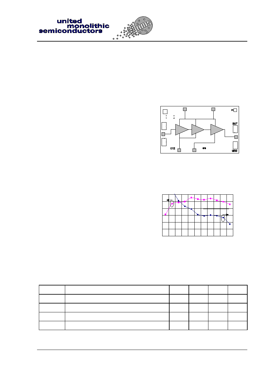
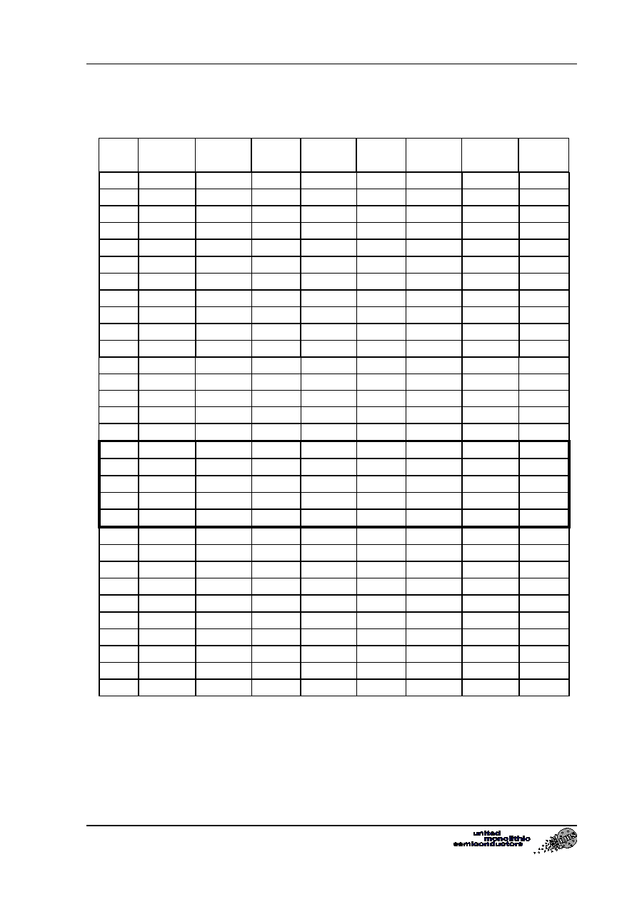
Typical Scattering Parameters ( On wafer Sij measurements )
Bias Conditions :
Vd = 3.5 Volt, Id = 60 mA.

Freq.
GHz
S11
dB
S11
/
/
/
/
S12
dB
S12
/
/
/
/
S21
dB
S21
/
/
/
/
S22
dB
S22
/
/
/
/
20,00 -2,75 120,50 -48,15 148,90 -29,86 60,85 -8,63 -167,63
21,00 -2,67 112,34 -47,38 124,38 -30,25 88,05 -8,34 -172,68
22,00 -2,61 103,14 -46,75 104,04 -27,37 109,54 -8,61 -179,98
23,00 -2,64 93,91 -47,13 86,03 -24,34 126,91 -8,92 172,06
24,00 -2,70 84,09 -47,59 78,03 -19,83 140,52 -9,57 163,86
25,00 -2,86 73,06 -47,20 57,56 -14,48 146,82 -10,03 156,11
26,00 -3,14 60,56 -48,55 43,27 -8,77 144,71 -10,82 146,54
27,00 -3,69 45,51 -51,10 30,27 -2,99 136,53 -12,09 136,06
28,00 -4,64 26,86 -53,09 53,09 3,00 121,47 -13,97 127,00
29,00 -6,67 1,63 -49,95 40,63 9,18 98,55 -17,34
120,22
30,00 -12,47 -33,41 -46,00 19,49 15,20 62,25 -22,38 145,19
31,00
-24,80 45,44 -42,45 -42,78 18,91 12,46 -16,56 167,67
32,00 -17,12 23,80 -41,43 -103,62 19,89 -32,13 -14,80 144,56
33,00 -23,20 -42,55 -40,56
-152,24 20,36 -67,68 -16,05 123,76
34,00 -19,03 -169,48 -39,68 170,39 20,77 -100,08 -18,09 107,73
35,00 -12,46 150,31 -38,71 143,10 20,98 -130,13 -21,69 77,58
36,00 -9,33 121,49 -37,54 123,52 21,06 -159,84 -27,59 9,57
37,00 -8,60 98,97 -36,14 104,39 20,87 172,52 -22,46 -82,68
38,00 -8,42 82,30 -34,82 83,69 20,58 146,27 -17,76 -110,30
39,00 -8,47 68,26 -33,60 64,74 20,27 121,22 -14,75 -129,22
40,00 -9,42 54,37 -32,98 45,70 19,84 95,76 -12,44 -146,78
41,00
-10,23 46,67 -32,48 26,65 19,24 72,14 -11,06
-164,32
42,00
-10,72 39,92 -32,21 11,28 18,67 50,20 -10,53
-179,35
43,00
-10,45 31,54 -31,68 -6,54 18,19 28,89 -10,41 170,06
44,00 -9,61 16,79 -31,02 -24,45 17,83 6,99 -10,02 160,92
45,00 -8,75 -4,98 -30,90 -42,39 17,42 -15,61 -9,83 151,98
46,00 -7,93 -30,22 -30,45 -61,72 17,00 -38,88 -9,17 144,58
47,00 -6,42 -61,17 -30,47 -83,47 16,37 -63,88 -8,39 134,96
48,00 -4,94 -93,19 -31,52 -107,28 15,28 -89,82 -7,55 121,85
49,00 -3,67 -122,84 -32,48 -128,35 13,83 -114,96 -6,98 108,11
50,00 -2,71 -147,44 -33,68 -147,17 12,15 -137,91 -6,69 91,01
CHA2394
36-40GHz Very Low Noise Amplifier
Ref. : DSCHA23942240 -28-Aug.-02
4/8
Specifications subject to change without notice
Route Dpartementale 128 , B.P.46 - 91401 ORSAY Cedex - FRANCE
Tel.: +33 (0)1 69 33 03 08 - Fax : +33 (0)1 69 33 03 09
Typical Output Power ( P-1dB gain compression ) Measurements.
( CW on wafer )


Conditions : Vd = 3.5 Volt, Frequency = 38 GHz.


Conditions : Id = 60 mA, Frequency = 38 GHz
.
4
6
8
10
12
14
16
18
20
22
20
30
40
50
60
70
80
90
100
Current Id ( mA )
Gai
n
& P-
1dB (
dB, dBm
)
Gain
P-1dB
4
6
8
10
12
14
16
18
20
22
2,5
3
3,5
4
4,5
Bias voltage Vd ( Volt )
Gai
n
& P-
1dB (
dB, dBm
)
Gain
P-1dB
36-40GHz Very Low Noise Amplifier
CHA2394
Ref. : DSCHA23942240 -28-Aug.-02
5/8
Specifications subject to change without notice
Route Dpartementale 128 , B.P.46 - 91401 ORSAY Cedex - FRANCE
Tel.: +33 (0)1 69 33 03 08 - Fax : +33 (0)1 69 33 03 09
Typical S parameters Measurements ( on wafer ).
Bias Conditions :
Vd = 3.5 Volt, Id = 60 mA.


Typical Gain &NF Measurements ( on wafer ).
Bias Conditions :
Vd = 3.5 Volt, Id = 60 mA.
10
12
14
16
18
20
22
30 31 32 33 34 35 36 37 38 39 40
Frequency (GHz)
Ga
i
n
(d
B
)
1
1,5
2
2,5
3
3,5
4
NF
(
d
B)
-20
-15
-10
-5
0
5
10
15
20
25
25
30
35
40
45
50
Frequency (GHz)
G
a
in
,
Rlo
s
s
(
d
B)
dBS11
dBS21
dBS22