CHA3092RBF
Ref. : DSCHA3092RBF2057 -26-Feb.-01-
1/8
Specifications subject to change without notice
United Monolithic Semiconductors S.A.S.
Route DÈpartementale 128 - B.P.46 - 91401 Orsay Cedex France
Tel. : +33 (0)1 69 33 03 08 - Fax : +33 (0)1 69 33 03 09
20-33GHz Medium Power Amplifier
GaAs Monolithic Microwave IC in SMD leadless package
Description
The monolithic microwave IC (MMIC) in the
package is a high gain broadband four-
stage monolithic medium power amplifier. It
is designed for a wide range of applications,
from military to commercial communication
systems. The circuit is manufactured with a
standard PM-HEMT process: 0.25µm gate
length, via holes through the substrate, air
bridges and electron beam gate lithography.
It is supplied in a new SMD leadless chip
carrier.
Main Features
Broad band performance: 20-33GHz
Gain = 20dB (typical)
Output power (P
-1dB
): 19dBm (typical)
Return loss < -6dB
Low DC power consumption, 300mA
SMD leadless package
Dimensions: 5.08 x 5.08 x 0.97 mm
3
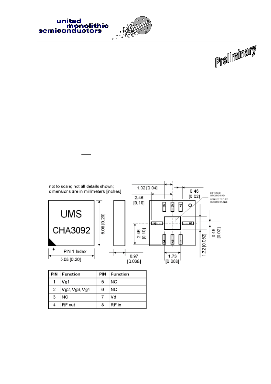
SMD Package Dimensions
"Please note that PIN 1 is located in the lower left corner of the package (front-side view) for all SMD-type packages from United Monolithic Semiconductors.
It is indicated by a triangle on the package lid. Starting with PIN 1 the other pads are numbered counter-clockwise (front-side view). ATTENTION: The dot on
the backside of the package (i.e. side with metallic pads) is just for fabrication purposes and does NOT indicate the location of PIN

CHA3092RBF
20-30GHz Medium Power Amplifier
Ref. : DSCHA3092RBF2057 -26-Feb.-01-
2/8
Specifications subject to change without notice
Route DÈpartementale 128 , B.P.46 - 91401 ORSAY Cedex - FRANCE
Tel.: +33 (0)1 69 33 03 08 - Fax : +33 (0)1 69 33 03 09
Schematic
Typical Bias Conditions
for an ambient Temperature of +25∞C
Symbol Pin
No.
Parameter
Values
Unit
Vd
7
Drain bias voltage
3.5
V
Vg1,2,3,4
1 & 2
First & second stages gate bias voltage
-0.2
V
Idd 7
Drain
current
300
mA
All other pins are not used for this device.
Absolute Maximum Ratings
Tamb. = 25∞C (1)
Symbol Parameter
Values
Unit
Vds
Drain bias voltage_small signal (2)
4.0
V
Ids
Drain bias current_small signal
400
mA
Vgs
Gate bias voltage
-2 to +0.4
V
Vdg
Negative Drain Gate voltage (= Vds ≠ Vgs)
+5
V
Pin
Maximum continuous input power (2)
Maximum peak input power overdrive (3)
+4
+15
dBm
dBm
Ta
Operating temperature range (4)
-40 to +85
∞C
Tstg
Storage temperature range
-55 to +155
∞C
(1) Operation of this device above anyone of these parameters may cause permanent damage.
(2) 3.5V recommended for up to a max of 3dB gain compression.
(3) Duration < 1s.
(4) Upper temperature limit strongly dependent on motherboard design; ratings given for
ideal thermal coupling

20-30GHz Medium Power Amplifier
CHA3092RBF
Ref. : DSCHA3092RBF2057 -26-Feb.-01-
3/8
Specifications subject to change without notice
Route DÈpartementale 128 , B.P.46 - 91401 ORSAY Cedex - FRANCE
Tel.: +33 (0)1 69 33 03 08 - Fax : +33 (0)1 69 33 03 09
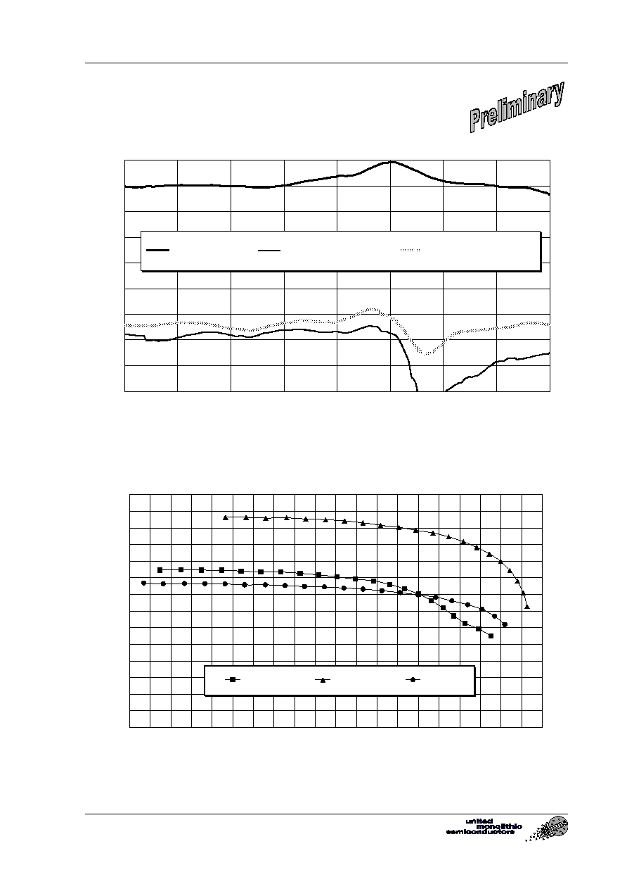
Typical results on PCB (recommended motherboard layout)
Vd=3.5V, Id adjusted at 300mA
Gain & Return Loss
-20
-15
-10
-5
0
5
10
15
20
25
18
20
22
24
26
28
30
32
34
frequency (GHz)
Linear Gain (dB)
Input Return Loss (dB)
Output Return Loss (dB)
Gain versus Output Power
10
11
12
13
14
15
16
17
18
19
20
21
22
23
24
3
4
5
6
7
8
9
10 11 12 13 14 15 16 17 18 19 20 21 22 23
Pout (dBm)
22GHz
28GHz
34GHz

CHA3092RBF
20-30GHz Medium Power Amplifier
Ref. : DSCHA3092RBF2057 -26-Feb.-01-
4/8
Specifications subject to change without notice
Route DÈpartementale 128 , B.P.46 - 91401 ORSAY Cedex - FRANCE
Tel.: +33 (0)1 69 33 03 08 - Fax : +33 (0)1 69 33 03 09
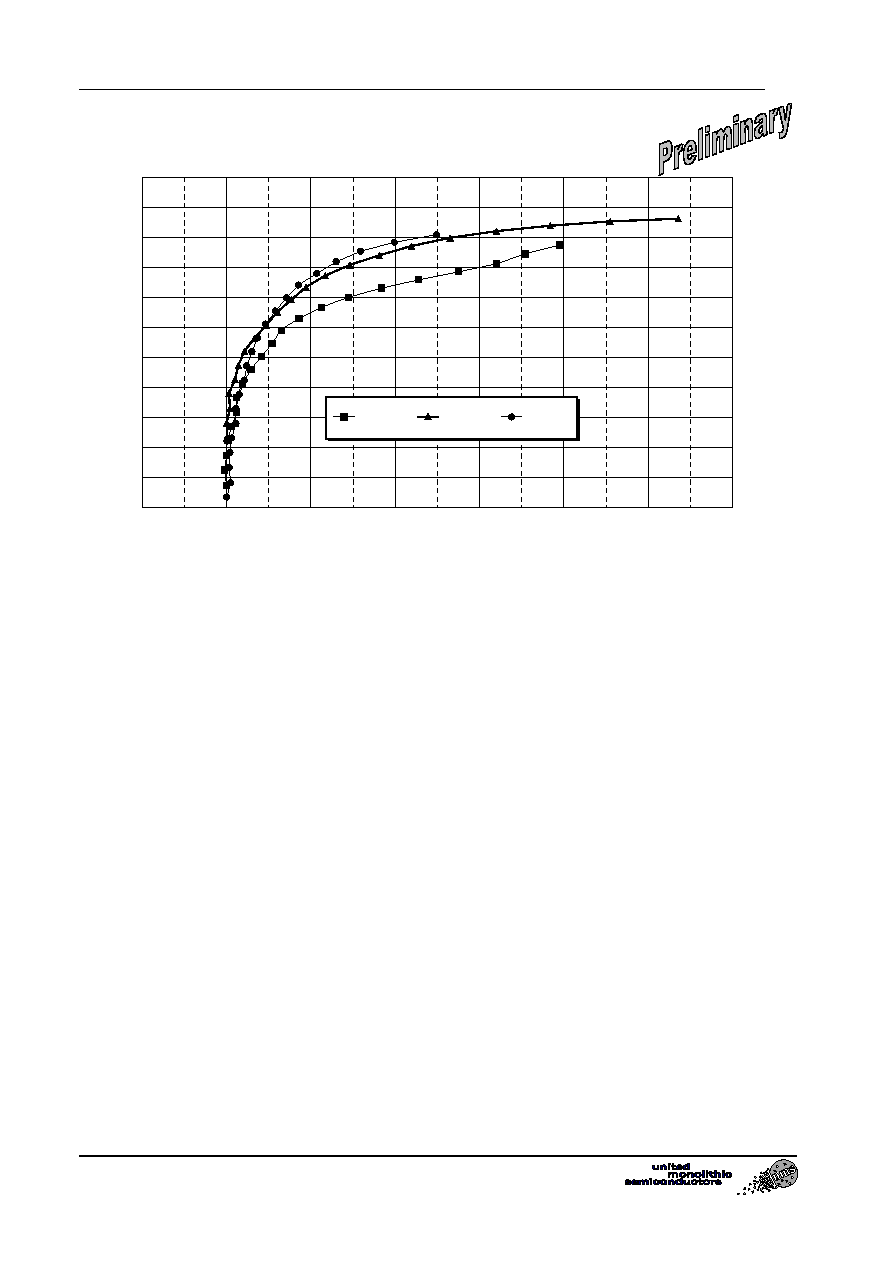
Output Power versus Gain Compression
3
5
7
9
11
13
15
17
19
21
23
25
-1
0
1
2
3
4
5
6
Gain compression (dB)
Ou
tput
pow
er
(
d
Bm
)
22GHz
28GHz
34GHz

20-30GHz Medium Power Amplifier
CHA3092RBF
Ref. : DSCHA3092RBF2057 -26-Feb.-01-
5/8
Specifications subject to change without notice
Route DÈpartementale 128 , B.P.46 - 91401 ORSAY Cedex - FRANCE
Tel.: +33 (0)1 69 33 03 08 - Fax : +33 (0)1 69 33 03 09
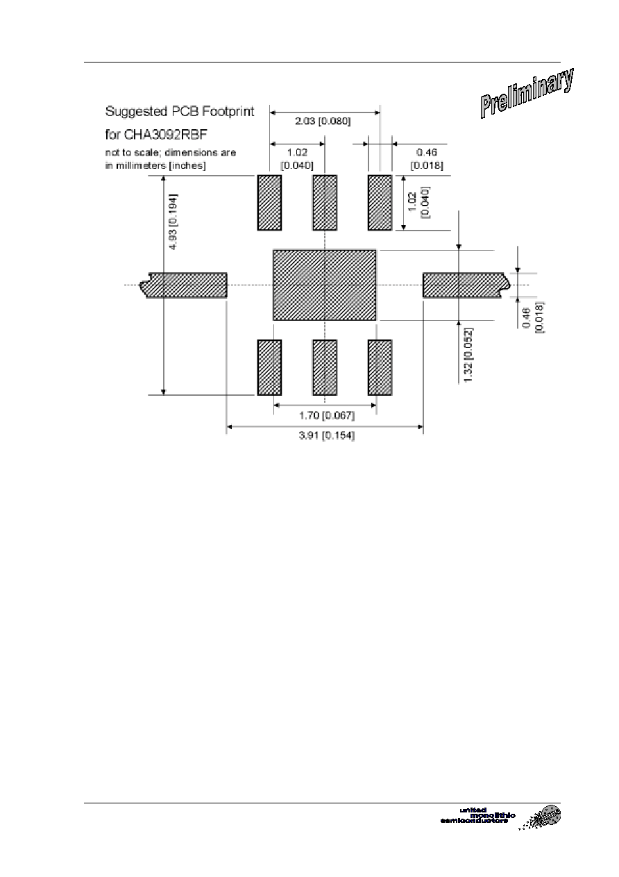
Footprint
