CHA4042
Ref. DSCHA4042345 - 14 feb 03
1/6
Specifications subject to change without notice
Route DÈpartementale 128 , B.P.46 - 91401 ORSAY Cedex - FRANCE
Tel.: +33 (0)1 69 33 03 08 - Fax : +33 (0)1 69 33 03 09
24-31 GHz Power Amplifier
GaAs Monolithic Microwave IC
Description
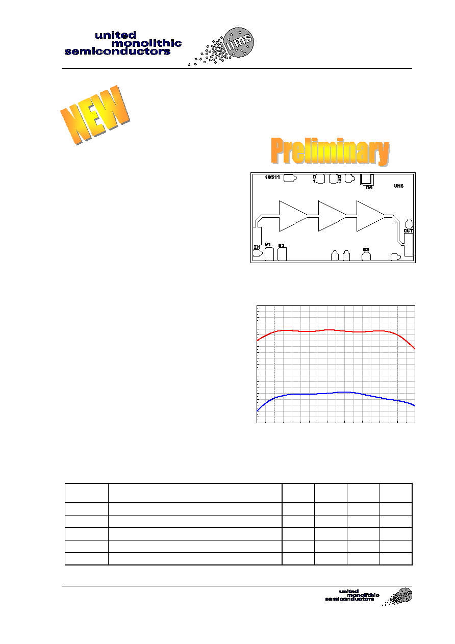
The CHA4042 is a compact three-stage
PHEMT HPA MMIC designed for point-to-point
multi-point radio, and other Ka-band
applications. It provides 25 dBm nominal output
power at 1dB gain compression over the 24-
31 GHz frequency range, and 15dB small signal
gain.
The circuit is manufactured with a 0.25µm gate
length power PHEMT process on 70-µm
substrate, via holes through the substrate, air
bridges and electron beam gate lithography.
It is available in chip form. The backside of the
chip is both RF and DC grounds. This helps to
simplify the assembly process.
Main Features
∑
Broadband performances : 24-31GHz
∑
15dB
±
1dB linear gain
∑
25.5dBm output power at 1-dB comp.
∑
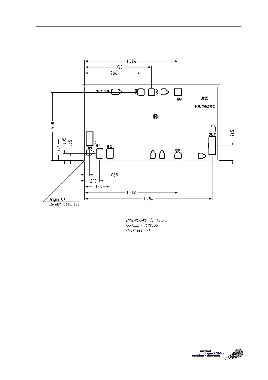
Chip size : 1.93 X 1.09 X 0.07mm
3
Chip size 2.1mm
2
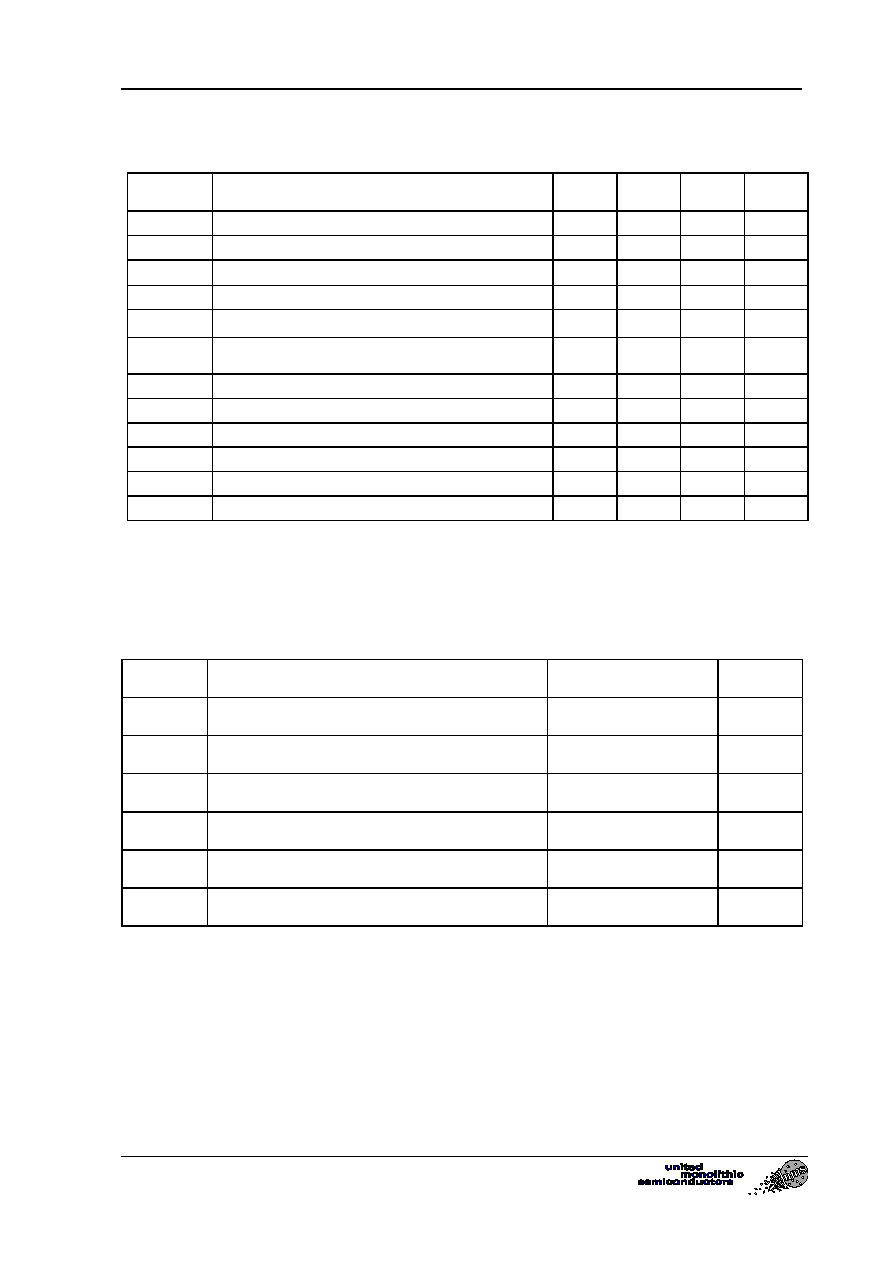
Main Characteristics
Tamb = +25∞C, Vd = 5V
Symbol Parameter Min
Typ
Max
Unit
Fop
Operating frequency range
24
31
GHz
G Small
signal
gain
14 15 dB
P1dB
CW output power at 1dB gain compression
25
25.5
dBm
Vd Drain
bias
voltage
5
V
Id Bias
current
250 500 mA
ESD Protection : Electrostatic discharge sensitive device. Observe handling precautions !
Typical MMIC characteristic
23
24
25
26
27
28
29
30
31
32
10
11
12
13
14
15
16
17
18
19
20
21
22
23
24
25
26
27
28
29
30
P
-1dB
CHA4042: V
d
=5 V, I
d
=250 mA
G
a
i
n
(
d
B
)
a
nd O
u
t
p
u
t
power
P
-1
d
B
(
d
B
m
)
Frequency (GHz)
Linear Gain
28.5-35 GHz POWER AMPLIFIER
CHA4042
Ref. : DSCHA4042345 - 14 feb 03
2/6
Specifications subject to change without notice
Route DÈpartementale 128 , B.P.46 - 91401 ORSAY Cedex - FRANCE
Tel.: +33 (0)1 69 33 03 08 - Fax : +33 (0)1 69 33 03 09
Electrical characteristics in JIG test fixture
Tamb = +25∞C, Vd = 5V, Id=250mA (typically Vg=-0.4V)
Symbol Parameter Min
Typ
Max
Unit
Fop
Operating frequency range
24
31
GHz
G
Small signal gain (1)
14
15
dB
G
Small signal gain flatness
±
1
dB
P1dB
CW output power at 1dB gain compression (2)
25
25.5
dBm
Psat
Saturated output power (1)
26
27
dBm
IP3 3
rd
order intercept point (1)
-
dBm
RLin
Input return loss (1)
-10
-9
dB
RLout
Output return loss (1)
-7
-5
dB
Is
Reverse Isolation (2)
40
dB
Vd Drain
bias
voltage
5
V
Id Bias
current
250 mA
Vg
Gate
bias
voltage
-0.4 V
(1)
These values are representative for CW JIG test fixture measurements, that are made with
bond wires at RF ports.
(2)
CW on-wafer measurements.
Absolute Maximum Ratings
(2)
Tamb = +25∞C
Symbol Parameter
Values
Unit
Vd
Drain bias voltage
6.5
V
Id
Maximum drain current
500
mA
Vg
Min. and max. gate bias voltage
-2.5 ~ 0
V
Pin
Maximum peak input power overdrive (3)
+15
dBm
Top
Operating temperature range
-40 to +85
∞C
Tstg
Storage temperature range
-55 to +125
∞C
(2) Operation of this device above anyone of these parameters may cause permanent damage.
(3) Duration < 1s.
28.5-35 GHz POWER AMPLIFIER
CHA4042
Ref. : DSCHA4042345 - 14 feb 03
3/6
Specifications subject to change without notice
Route DÈpartementale 128 , B.P.46 - 91401 ORSAY Cedex - FRANCE
Tel.: +33 (0)1 69 33 03 08 - Fax : +33 (0)1 69 33 03 09
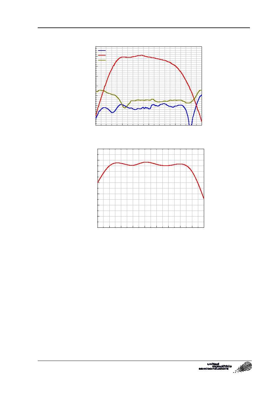
Typical CW performance @ Tamb=25∞C
20
25
30
35
40
-20
-15
-10
-5
0
5
10
15
20
CHA4042: V
d
=5 V, I
d
=250 mA
S Par
a
met
e
rs
(
d
B
)
Frequency (GHz)
S
11
S
21
S
22
Typical JIG test fixture S-parameter measurements (test fixture losses uncorrected)
23
24
25
26
27
28
29
30
31
32
20
21
22
23
24
25
26
27
CHA4042: V
d
=5 V, I
d
=250 mA
Out
p
u
t
po
w
e
r
a
t
1-
dB c
o
m
p
r
e
ss
i
o
n (
d
Bm
)
Frequency (GHz)
Typical CW output power at 1-dB gain compression (on-wafer measurements)
28.5-35 GHz POWER AMPLIFIER
CHA4042
Ref. : DSCHA4042345 - 14 feb 03
4/6
Specifications subject to change without notice
Route DÈpartementale 128 , B.P.46 - 91401 ORSAY Cedex - FRANCE
Tel.: +33 (0)1 69 33 03 08 - Fax : +33 (0)1 69 33 03 09
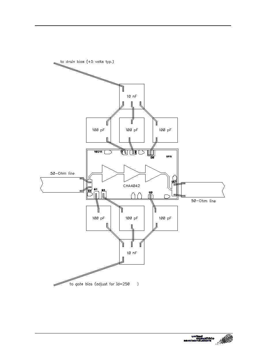
Chip Assembly and Mechanical Data
mA
28.5-35 GHz POWER AMPLIFIER
CHA4042
Ref. : DSCHA4042345 - 14 feb 03
5/6
Specifications subject to change without notice
Route DÈpartementale 128 , B.P.46 - 91401 ORSAY Cedex - FRANCE
Tel.: +33 (0)1 69 33 03 08 - Fax : +33 (0)1 69 33 03 09
Bonding pad positions