 | –≠–ª–µ–∫—Ç—Ä–æ–Ω–Ω—ã–π –∫–æ–º–ø–æ–Ω–µ–Ω—Ç: CHA5042 | –°–∫–∞—á–∞—Ç—å:  PDF PDF  ZIP ZIP |

CHA5042
Ref. : DSCHA50422218 -06-Aug.-02
1
/6
Specifications subject to change without notice
United Monolithic Semiconductors S.A.S.
Route DÈpartementale 128 - B.P.46 - 91401 Orsay Cedex France
Tel. : +33 (0)1 69 33 03 08 - Fax : +33 (0)1 69 33 03 09
13≠16GHz High Power Amplifier
GaAs Monolithic Microwave IC
Description
The CHA5042 is a three-stage pHEMT
HPA MMIC designed for VSAT ground
terminals and other radio applications. The
CHA5042 provides 29.5dBm nominal
output power at 1dB gain compression
over the 13-16GHz frequency range, and
26dB small-signal gain. This product will be
available in chip form.
Main Features
æ
Frequency Range:
13-16GHz
æ
Gain:
26dB
æ
Output Power (P-1dB): 29.5dBm
æ
Output TOI:
37.5dBm
æ
Input Return Loss:
15dB
æ
Output Return Loss:
15dB
æ
Bias:
9V,
0.4A
æ
Dimensions: 1.37 x 1.33 x 0.07 mm
Predicted Gain & Return
5
10
15
20
25
30
11
12
13
14
15
16
17
18
FREQUENCY (GHz)
S.
S
.
G
A
IN
(
d
B
)
-25
-20
-15
-10
-5
0
GAIN (dB)
Input Return Loss (dB)
Output Return
Loss (dB)

CHA5042
13-16GHz High Power Amplifier
Ref. : DSCHA50422218 -06-Aug.-02
2/6
Specifications subject to change without notice
Route DÈpartementale 128 , B.P.46 - 91401 ORSAY Cedex - FRANCE
Tel.: +33 (0)1 69 33 03 08 - Fax : +33 (0)1 69 33 03 09
Predicted Output Power at 1dB Gain compression
Symbol
Parameter
Values
Unit
Vds
Drain bias voltage_small signal
10.5
V
Ids
Drain bias current_small signal
650
mA
Vgs
Gate bias voltage
-2 to +0.4
V
Vdg
Maximum Drain Gate voltage (Vd-Vg)
+12
V
Pin
Maximum peak input power overdrive (2)
+18
dBm
Ta
Operating Temperature Range (3)
-45 to +80
C
Tstg
Storage Temperature Range
-55 to +125
C
∑
Operation of this device above any one of these parameters may cause
permanent damage.
∑
Duration < 1 s
∑
AuSn solder mount to CuW or CuMo carrier assumed
27
27.5
28
28.5
29
29.5
30
30.5
31
31.5
32
12
13
14
15
16
17
FREQUENCY (GHz)
OU
T
P
U
T
P
O
W
E
R
(P
-1d
B
) (d
B
m
)
13-16GHz High Power Amplifier
CHA5042
Ref. : DSCHA50422218 -06-Aug.-02
3
/6
Specifications subject to change without notice
Route DÈpartementale 128 , B.P.46 - 91401 ORSAY Cedex - FRANCE
Tel.: +33 (0)1 69 33 03 08 - Fax : +33 (0)1 69 33 03 09
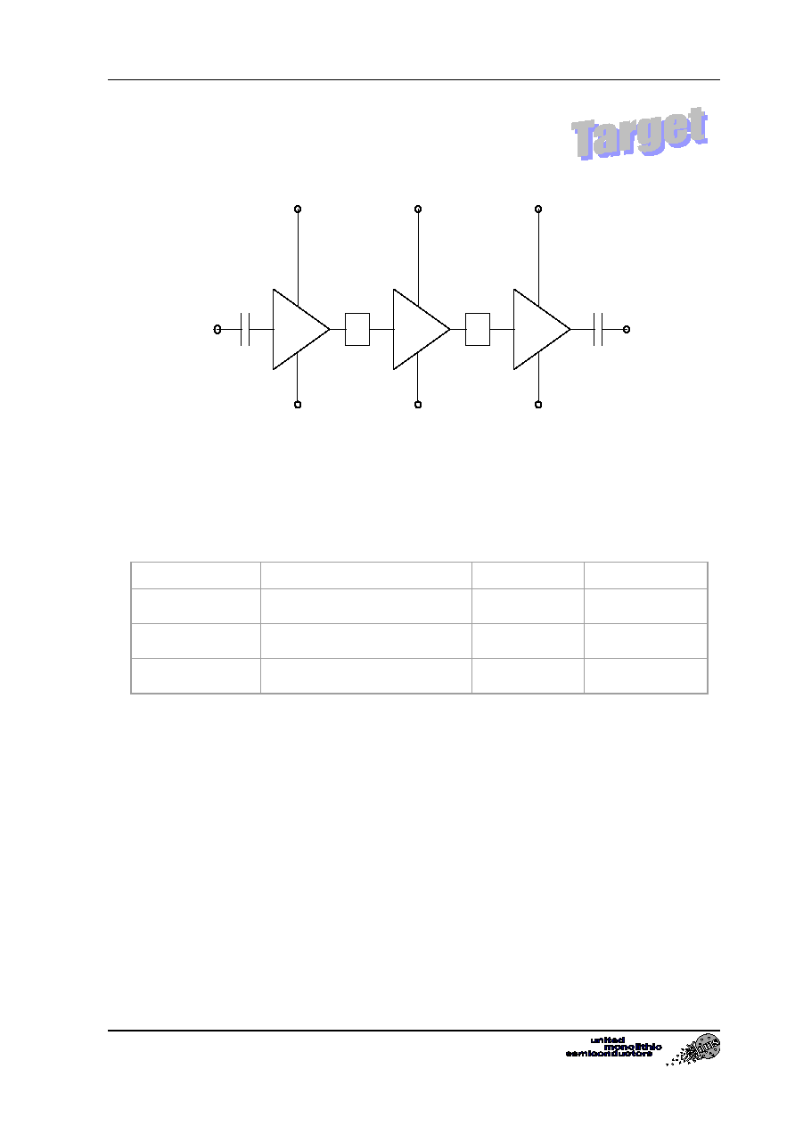
Schematic
Symbol
Parameter
Values
Unit
Vd 1, 2, 3
Drain bias voltage
9.0
V
Vg 1, 2, 3
Gate bias voltage
-0.5
V
Idd
Total drain current
400
mA
RF
RF Out
Vd1
Vd2
Vd3
Vg1
Vg2
Vg3
Typical Bias Conditions
Tamb. = 25
∞
C

CHA5042
13-16GHz High Power Amplifier
Ref. : DSCHA50422218 -06-Aug.-02
4/6
Specifications subject to change without notice
Route DÈpartementale 128 , B.P.46 - 91401 ORSAY Cedex - FRANCE
Tel.: +33 (0)1 69 33 03 08 - Fax : +33 (0)1 69 33 03 09
MMIC Outline & Bond Pads
Not to scale, dimensions are in millimeters
1.37
±
0.35
1.33
±
0.35
1
2 3
4
5
6
7
8
(0, 0)
Bond Pad
Symbol
x-dim.
y-dim.
x-center
y-center
(um)
(um)
(um)
(um)
1
RF input
100
200
100
820
2
Vd1
100
100
285
1230
3
Vd2
100
90
450
1230
4
Vd3
100
100
1120
1235
5
RF output
100
200
1285
790
6
Vg3
100
100
1280
155
7
Vg2
100
100
895
105
8
Vg1
100
100
505
105
Chip size : 1370µm +/-35µm x 1330µm +/- 35µm
13-16GHz High Power Amplifier
CHA5042
Ref. : DSCHA50422218 -06-Aug.-02
5
/6
Specifications subject to change without notice
Route DÈpartementale 128 , B.P.46 - 91401 ORSAY Cedex - FRANCE
Tel.: +33 (0)1 69 33 03 08 - Fax : +33 (0)1 69 33 03 09
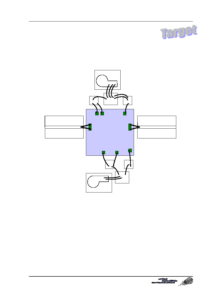
MMIC Assembly and Bonding Diagram ( not to scale )
VD1 VD2
VD3
R
F
O
U
R
F
IN
VG1
VG2
VG3
V
g
100p
0.01µ
100p
V
D
100p
0.01µ
100p
50 Ohm line
50 Ohm line
RFin
RFout