CHA5042
Ref. : DSCHA50423141 - 21 May 03
1/6
Specifications subject to change without notice
Route DÈpartementale 128 , B.P.46 - 91401 ORSAY Cedex - FRANCE
Tel.: +33 (0)1 69 33 03 08 - Fax : +33 (0)1 69 33 03 09
13-17 GHz Power Amplifier
GaAs Monolithic Microwave IC
Description
The CHA5042 is a compact three-stage
PHEMT HPA MMIC designed for VSAT ground
terminals and other radio applications. It
provides typically more than 27dBm nominal
output power at 1dB gain compression over the
13-17 GHz frequency range, and 28.5dB small
signal gain.
The circuit is manufactured with a 0.25µm gate
length power PHEMT process on 70µm
substrate, via holes through the substrate, air
bridges and electron beam gate lithography.
It is available in 10-lead flange package form.
The backside of the package is both RF and DC
grounds. This helps to simplify the assembly
process.
Main Features
∑
Broadband performances : 13-17GHz
∑
28dB
±
3dB linear gain
∑
>27dBm output power at 1dB comp
13
14
15
16
17
10
15
20
25
30
35
P
-1dB
CHA5042: V
d
=8 V, I
d
=310 mA
G
a
in
(d
B)
and
ou
tput
p
o
wer
(d
Bm)
Frequency (GHz)
Gain
Main Characteristics
Tamb = +25∞C, Vd = 8V
Symbol Parameter Min
Typ
Max
Unit
Fop
Operating frequency range
13
17
GHz
G Small
signal
gain
25.5 28 dB
P1dB
CW output power at 1dB gain compression
27
28
dBm
Vd Drain
bias
voltage
8
V
Id Quiescent
bias
current
310 mA
ESD Protection : Electrostatic discharge sensitive device. Observe handling precautions !

CHA5042
Ref. : DSCHA50423141 - 21 May 03
2/6
Specifications subject to change without notice
Route DÈpartementale 128 , B.P.46 - 91401 ORSAY Cedex - FRANCE
Tel.: +33 (0)1 69 33 03 08 - Fax : +33 (0)1 69 33 03 09
Electrical characteristics in JIG test fixture
Tamb = +25∞C, Vd = 8V, Id=310mA (typically Vg=-0.45V)
Symbol Parameter Min
Typ
Max
Unit
Fop
Operating frequency range
13
17
GHz
G
Small signal gain (1)
25.5
28
dB
G
Small signal gain flatness
±
3
dB
P1dB
CW output power at 1dB gain compression (1)
27
28
dBm
Psat
Saturated output power (1)
29
dBm
RLin
Input return loss (1)
-10
dB
RLout
Output return loss (1)
-10
dB
Is
Reverse Isolation (1)
40
dB
Vd
Drain bias voltage (2)
8
9
V
Id
Bias current (2)
310
400
mA
Ig Gate
current
5 mA
Vg Gate
bias
voltage
-0.45 V
(1)
These values are representative for CW measurements in test fixture and do not include test
fixture losses (corrected measurements).
(2)
One may adjust from 8V/310 mA to 9V/400mA to increase output power by approx. 1dB
Absolute Maximum Ratings
(2)
Tamb = +25∞C
Symbol Parameter
Values
Unit
Vd
Drain bias voltage
9.5
V
Id
Maximum bias current
500
mA
Vg
Min. and max. gate bias voltage
-2.5 ~ 0
V
Pin
Maximum peak input power overdrive (3)
+3
dBm
Top
Operating temperature range
-40 to +85
∞C
Tstg
Storage temperature range
-55 to +125
∞C
(2) Operation of this device above anyone of these parameters may cause permanent damage.
(3) Duration < 1s.

13-17 GHz POWER AMPLIFIER
CHA5042
Ref. : DSCHA50423141 - 21 May 03
3/6
Specifications subject to change without notice
Route DÈpartementale 128 , B.P.46 - 91401 ORSAY Cedex - FRANCE
Tel.: +33 (0)1 69 33 03 08 - Fax : +33 (0)1 69 33 03 09
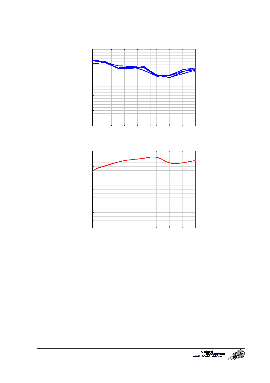
Typical CW performance @ Tamb=25∞C
13
14
15
16
17
10
15
20
25
30
35
CHA5042-MFF: P
in
=-20 dBm, V
d
=8 V, I
d
=310 mA
S
m
al
l
s
i
g
nal
gai
n
(
d
B
)
Frequency (GHz)
Typical test fixture small signal gain at V
d
=8 V and I
d
=310 mA (5 samples)
13
14
15
16
17
20
21
22
23
24
25
26
27
28
29
30
CHA5042: V
d
=8 V, I
d
=310 mA
O
u
t
p
u
t
pow
er
at
1-d
B
gai
n co
mpr
e
ss
i
o
n (d
B
m
)
Frequency (GHz)
Typical test fixture output power at 1-dB gain compression at V
d
=8 V and I
d
=310 mA

13-17 GHz POWER AMPLIFIER
CHA5042
Ref. : DSCHA50423141 - 21 May 03
4/6
Specifications subject to change without notice
Route DÈpartementale 128 , B.P.46 - 91401 ORSAY Cedex - FRANCE
Tel.: +33 (0)1 69 33 03 08 - Fax : +33 (0)1 69 33 03 09
-20
-15
-10
-5
0
5
5
10
15
20
25
30
13 GHz
14 GHz
15 GHz
16 GHz
17 GHz
CHA5042: V
d
=8 V
Ou
tp
u
t
P
o
w
e
r (d
B
m
)
Input power (dBm)
Typical test fixture output power versus input power at V
d
=8 V and I
d
=310 mA
-20
-15
-10
-5
0
200
220
240
260
280
300
320
340
360
380
400
13 GHz
14 GHz
15 GHz
16 GHz
17 GHz
CHA5042: V
d
=8 V
Dr
ai
n
cu
rr
en
t
(m
A
)
Input power (dBm)
Typical bias current versus input power at V
d
=8 V and I
d
=310 mA

13-17 GHz POWER AMPLIFIER
CHA5042
Ref. : DSCHA50423141 - 21 May 03
5/6
Specifications subject to change without notice
Route DÈpartementale 128 , B.P.46 - 91401 ORSAY Cedex - FRANCE
Tel.: +33 (0)1 69 33 03 08 - Fax : +33 (0)1 69 33 03 09
Chip Assembly and Mechanical Data
Units = mm
Pin-reference:
1 - Vd
6 - Vg
2 - GND
7 - GND
3 - RFin
8 - RFout
4 - GND
9 - GND
5 - Vg
10 - Vd
CH
A50
4
2


