CHA5093TCF
Ref. : DSCHA50932035 - 04-Feb.-02
1/6
Specifications subject to change without notice
United Monolithic Semiconductors S.A.S.
Route DÈpartementale 128 - B.P.46 - 91401 Orsay Cedex France
Tel. : +33 (0)1 69 33 03 08 - Fax : +33 (0)1 69 33 03 09
24-26GHz High Power Amplifier
GaAs Monolithic Microwave IC in SMD leadless package
Description
The packaged monolithic microwave IC
(MMIC) is a high gain three-stage
monolithic high power amplifier. It is
designed for a wide range of applications,
from military to commercial communication
systems.
The circuit is manufactured with a PM-
HEMT process, 0.25µm gate length, via
holes through the substrate, air bridges and
electron beam gate lithography. It is
supplied in a new SMD leadless chip
carrier.
Main Features
Performances: 24-26GHz
Gain = 19dB (typical)
Output power (P
-1dB
) 29dBm (typical)
SMD leadless package
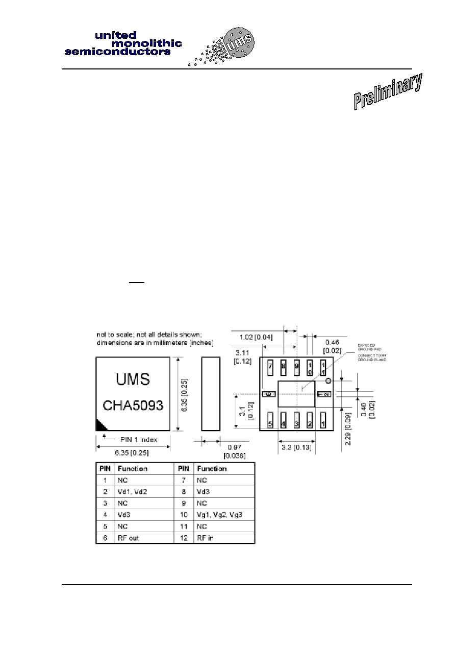
Dimensions: 6.35 x 6.35 x 0.97 mm
3
SMD Package Dimensions
"Please note that PIN 1 is located in the lower left corner of the package (front-side view) for all SMD-type packages from United Monolithic Semiconductors.
It is indicated by a triangle on the package lid. Starting with PIN 1 the other pads are numbered counter-clockwise (front-side view). ATTENTION: The dot on
the backside of the package (i.e. side with metallic pads) is just for fabrication purposes and does NOT indicate the location of PIN
CHA5093TCF
24-26GHz High Power Amplifier
Ref. : DSCHA50932035 - 04-Feb.-02
2/6
Specifications subject to change without notice
Route DÈpartementale 128 , B.P.46 - 91401 ORSAY Cedex - FRANCE
Tel.: +33 (0)1 69 33 03 08 - Fax : +33 (0)1 69 33 03 09
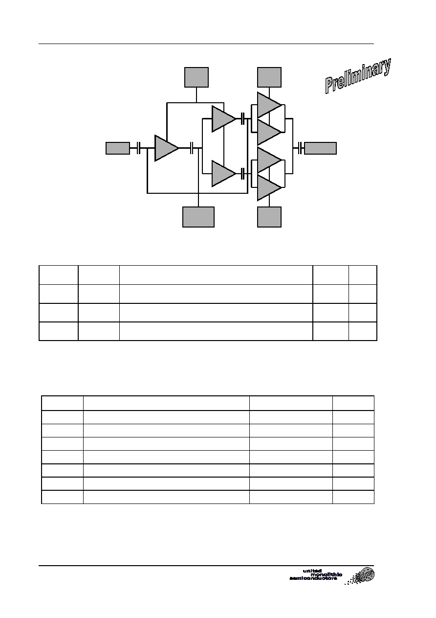
Schematic
Typical Bias Conditions
for an ambient Temperature of +25∞C
Symbol Pin
No.
Parameter
Values Unit
Vd1,2,3
2, 4 & 8
Drain bias voltage
6
V
Vg1,2,3
10
First, second & third stages gate bias voltage
-0.4
V
Idd
2,4 & 8
Total drain current
600
mA
All other pins are not used for this device.
Absolute Maximum Ratings
Tamb. = 25∞C (1)
Symbol Parameter
Values
Unit
Vds
Drain bias voltage_small signal
6.0
V
Ids
Drain bias current_small signal
1200
mA
Vgs
Gate bias voltage
-2 to +0.4
V
Vdg
Negative Drain Gate voltage (= Vds ≠ Vgs)
+8
V
Pin
Maximum peak input power overdrive (3)
+12
dBm
Ta
Operating temperature range (4)
-40 to +70
∞C
Tstg
Storage temperature range
-55 to +155
∞C
(1) Operation of this device above anyone of these parameters may cause permanent damage.
(2) 6V recommended for up to a max of 1dB gain compression.
(3) Duration < 1s.
(4) Upper temperature limit strongly dependent on motherboard design; ratings given for
ideal thermal coupling
RF IN
RF OUT
Vd1,2
CHA5093TCF
Vg1,2,3
Vd3
Vd3
RF IN
RF OUT
Vd1,2
CHA5093TCF
Vg1,2,3
Vd3
Vd3
24-26GHz High Power Amplifier
CHA5093TCF
Ref. : DSCHA50932035 - 04-Feb.-02
3/6
Specifications subject to change without notice
Route DÈpartementale 128 , B.P.46 - 91401 ORSAY Cedex - FRANCE
Tel.: +33 (0)1 69 33 03 08 - Fax : +33 (0)1 69 33 03 09
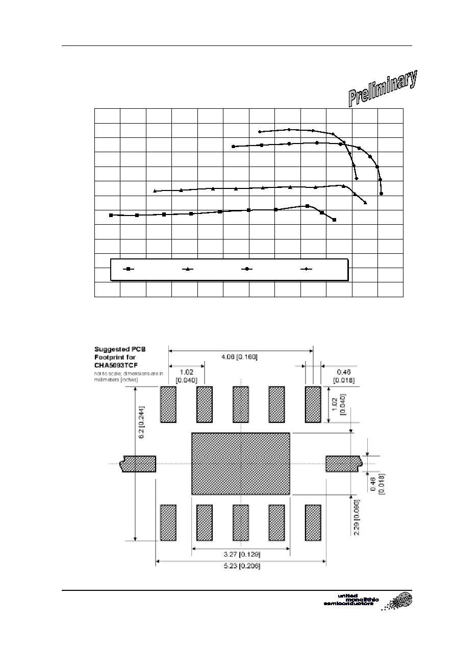
Typical results on PCB (recommended motherboard layout)
Vd=6V, Id adjusted at 600mA
Gain versus output power
10
11
12
13
14
15
16
17
18
19
20
21
22
23
20
21
22
23
24
25
26
27
28
29
30
31
32
Pout (dBm)
Ga
i
n
(
d
B
)
23GHz
24GHz
25GHz
26GHz
Footprint
CHA5093TCF
24-26GHz High Power Amplifier
Ref. : DSCHA50932035 - 04-Feb.-02
4/6
Specifications subject to change without notice
Route DÈpartementale 128 , B.P.46 - 91401 ORSAY Cedex - FRANCE
Tel.: +33 (0)1 69 33 03 08 - Fax : +33 (0)1 69 33 03 09
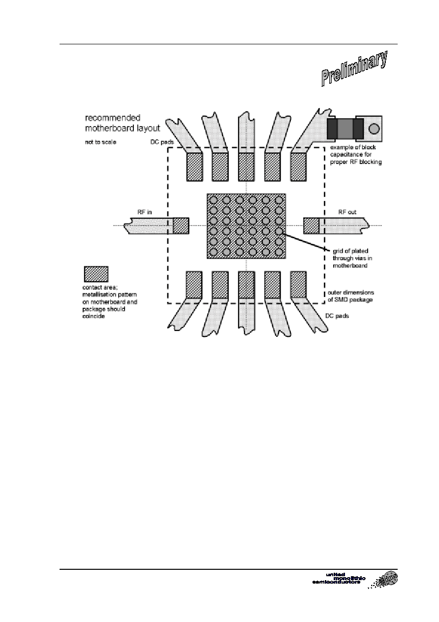
Application note
The design of the motherboard has a strong impact on the over all performance
since the transition from the motherboard to the package is comparably large. In
case of the SMD type packages of United Monolithic Semiconductors the
motherboard should be designed according to the information given in the following
to achieve good performance. Other configurations are also possible but can lead to
different results. If you need advise please contact United Monolithic Semiconductors
for further information.
SMD type packages of UMS should allow design and fabrication of micro- and mm-
wave modules at low cost. Therefore, a suitable motherboard environment has been
chosen. All tests and verifications have been performed on Rogers RO4003. This
material exhibits a permittivity of 3.38 and has been used with a thickness of 200µm
[8 mils] and a 1/2oz or less copper cladding. The corresponding 50 Ohm
transmission line has a strip width of about 460µm [approx. 18 mils].
The contact areas on the motherboard for the package connections should be
designed according to the footprint given above. The proper via structure under the
ground pad is very important in order to achieve a good RF and lifetime
performance. All tests have been done by using a grid of plenty plated through vias
with a diameter of less than 200µm [8 mils] and a spacing of less than 400µm [16
mils] from the centres of two adjacent vias. The via grid should cover the whole
space under the ground pad and the vias closest to the RF ports should be located
near the edge of the pad to allow a good RF ground connection. Since the vias are
important for heat transfer, a proper via filling should be guaranteed during the
mounting procedure to get a low thermal resistance between package and heat sink.
For power devices the use of heat slugs in the motherboard instead of a via grid is
recommended.
For the mounting process the SMD type package can be handled as a standard
surface mount component. The use of either solder or conductive epoxy is possible.
The solder thickness after reflow should be typical 50µm [2 mils] and the lateral
alignment between the package and the motherboard should be within 50µm [2
mils]. Caution should be taken to obtain a good and reliable contact over the whole
pad areas. Voids or other improper connections, in particular, between the ground
pads of motherboard and package will lead to a deterioration of the RF performance
and the heat dissipation. The latter effect can reduce drastically reliability and lifetime
of the product.
24-26GHz High Power Amplifier
CHA5093TCF
Ref. : DSCHA50932035 - 04-Feb.-02
5/6
Specifications subject to change without notice
Route DÈpartementale 128 , B.P.46 - 91401 ORSAY Cedex - FRANCE
Tel.: +33 (0)1 69 33 03 08 - Fax : +33 (0)1 69 33 03 09
The RF ports comprise a DC blocking capacitor on chip level. The DC connections
include a first level of DC decoupling capacitors (typically 120pF) in the package.
However, all DC bias ports should be additionally connected to ground with 10nF
capacitors at board level to prevent the MMIC from oscillations. These parts should
be placed close to the SMD leadless package. If the same bias is required at
different DC ports, the lines should only be connected behind these block capacitors.
Further information on the application of the SMD leadless packages for GaAs
monolithic microwave ICs are given in the UMS Application Note AN0005.