
CHA5290
Ref. DSCHA52902295 -22-Oct.-02
1/6
Specifications subject to change without notice
United Monolithic Semiconductors S.A.S.
Route DÈpartementale 128 - B.P.46 - 91401 Orsay Cedex France
Tel. : +33 (0)1 69 33 03 08 - Fax : +33 (0)1 69 33 03 09
17.7-24GHz Medium Power Amplifier
GaAs Monolithic Microwave IC
Description
The CHA5290 is a high gain four-stage
monolithic medium power amplifier. It is
designed for a wide range of applications, from
military to commercial communication
systems. The backside of the chip is both RF
and DC grounds. This helps simplify the
assembly process.
The circuit is manufactured with a PM-HEMT
process, 0.25µm gate length, via holes through
the substrate, air bridges and electron beam
gate lithography.
It is available in chip form.
Main Features
Performances : 17.7 -24GHz
26dBm output power @ 1dB comp. gain
26 dB
±
1dB gain
DC power consumption, 400mA @ 6V
Chip size : 3.43 x 1.57 x 0.05 mm
Vd1 Vd2 Vd3 Vd4
Vg1,2 Vg3 Vg4 Vd4
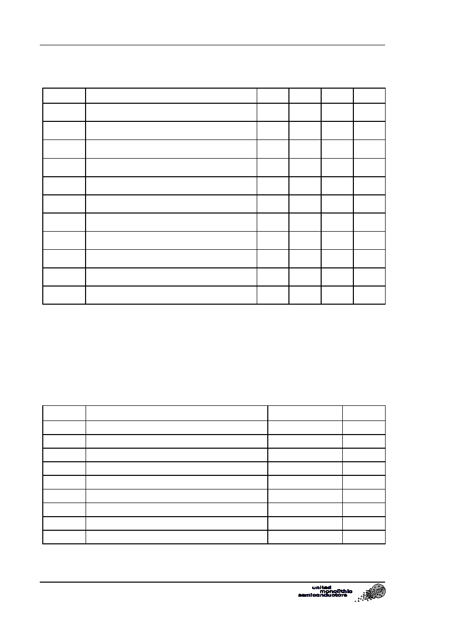
Typical on jig Measurements
Main Characteristics
Tamb. = 25∞C
Symbol Parameter Min
Typ
Max
Unit
Fop
Operating frequency range
17.7
24
GHz
G
Small signal gain
26
dB
P1dB
Output power at 1dB gain compression
26
dBm
Id Bias
current
400
mA
ESD Protection : Electrostatic discharge sensitive device. Observe handling precautions !
-30
-26
-22
-18
-14
-10
-6
-2
2
6
10
14
18
22
26
30
34
14
16
18
20
22
24
26
28
30
32
34
Frequency (GHz)
S11 (dB)
S21 (dB)
S22 (dB)
CHA5290
18-24GHz Medium Power Amplifier
Ref. DSCHA52902295 -22-Oct.-02
2/6
Specifications subject to change without notice
Route DÈpartementale 128 , B.P.46 - 91401 ORSAY Cedex - FRANCE
Tel.: +33 (0)1 69 33 03 08 - Fax : +33 (0)1 69 33 03 09
Electrical Characteristics
Tamb = +25∞C, Vd = 6V Id =400mA
Symbol Parameter Min
Typ
Max
Unit
Fop
Operating frequency range (1)
17.7
24
GHz
G
Small signal gain (1)
24
26
dB
G
Small signal gain flatness (1)
±
1
dB
Is
Reverse isolation
40
dB
P1dB
Pulsed output power at 1dB compression (1)
25
26
dBm
P03
Output power at 3dB gain compression (1)
27
dBm
PAE
Power added efficiency at 1dB comp.
18
%
VSWRin Input VSWR (2)
3:1
VSWRout Output VSWR (2)
3:1
Tj
Junction temperature for 80∞C backside
165
∞C
Id
Bias current @ small signal
400
500
mA
(1) These values are representative for pulsed on-wafer measurements that are made without
bonding wires at the RF ports.
(2) Value representative for CW on jig measurement.
Absolute Maximum Ratings
Tamb. = 25∞C (1)
Symbol Parameter
Values
Unit
Vd
Maximum drain bias voltage with Pin max=-2dBm
6.25
V
Id
Maximum drain bias current
625
mA
Vg
Gate bias voltage
-2.5 to +0.4
V
Ig
Gate bias current
-2.5 to +2.5
mA
Vgd
Minimum negative gate drain voltage ( Vg - Vd)
-8
V
Pin
Maximum input power overdrive (2)
3
dBm
Tch
Maximum channel temperature
175
∞C
Ta
Operating temperature range
-40 to +80
∞C
Tstg
Storage temperature range
-55 to +125
∞C
(1) Operation of this device above anyone of these parameters may cause permanent damage.
(2) Duration < 1s.
18-24GHz Medium Power Amplifier
CHA5290
Ref. DSCHA52902295 -22-Oct.-02
3/6
Specifications subject to change without notice
Route DÈpartementale 128 , B.P.46 - 91401 ORSAY Cedex - FRANCE
Tel.: +33 (0)1 69 33 03 08 - Fax : +33 (0)1 69 33 03 09
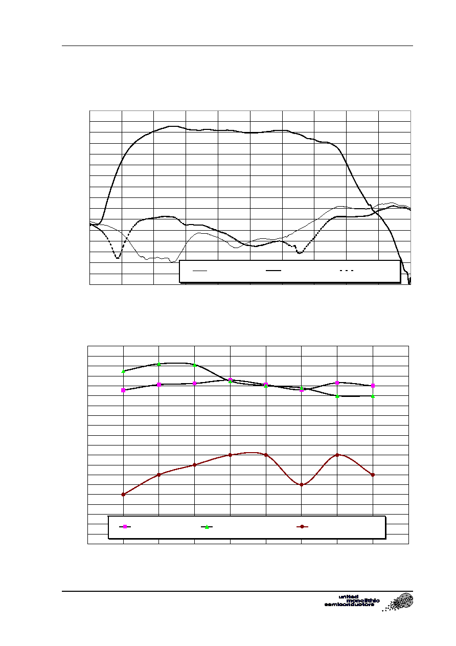
Typical on Jig Measurements
Bias conditions: Vd=6V, Vg tuned for Id = 400mA
Linear Gain & Return Losses versus frequency
Linear Gain, Output power & associated PAE at 1dB compression versus frequency
-30
-26
-22
-18
-14
-10
-6
-2
2
6
10
14
18
22
26
30
34
14
16
18
20
22
24
26
28
30
32
34
Frequency (GHz)
S11 (dB)
S21 (dB)
S22 (dB)
10
11
12
13
14
15
16
17
18
19
20
21
22
23
24
25
26
27
28
29
30
16
17
18
19
20
21
22
23
24
25
Frequency (GHz)
P-1dB (dBm)
Linear Gain (dB)
PAE@ 1dB comp.
CHA5290
18-24GHz Medium Power Amplifier
Ref. DSCHA52902295 -22-Oct.-02
4/6
Specifications subject to change without notice
Route DÈpartementale 128 , B.P.46 - 91401 ORSAY Cedex - FRANCE
Tel.: +33 (0)1 69 33 03 08 - Fax : +33 (0)1 69 33 03 09
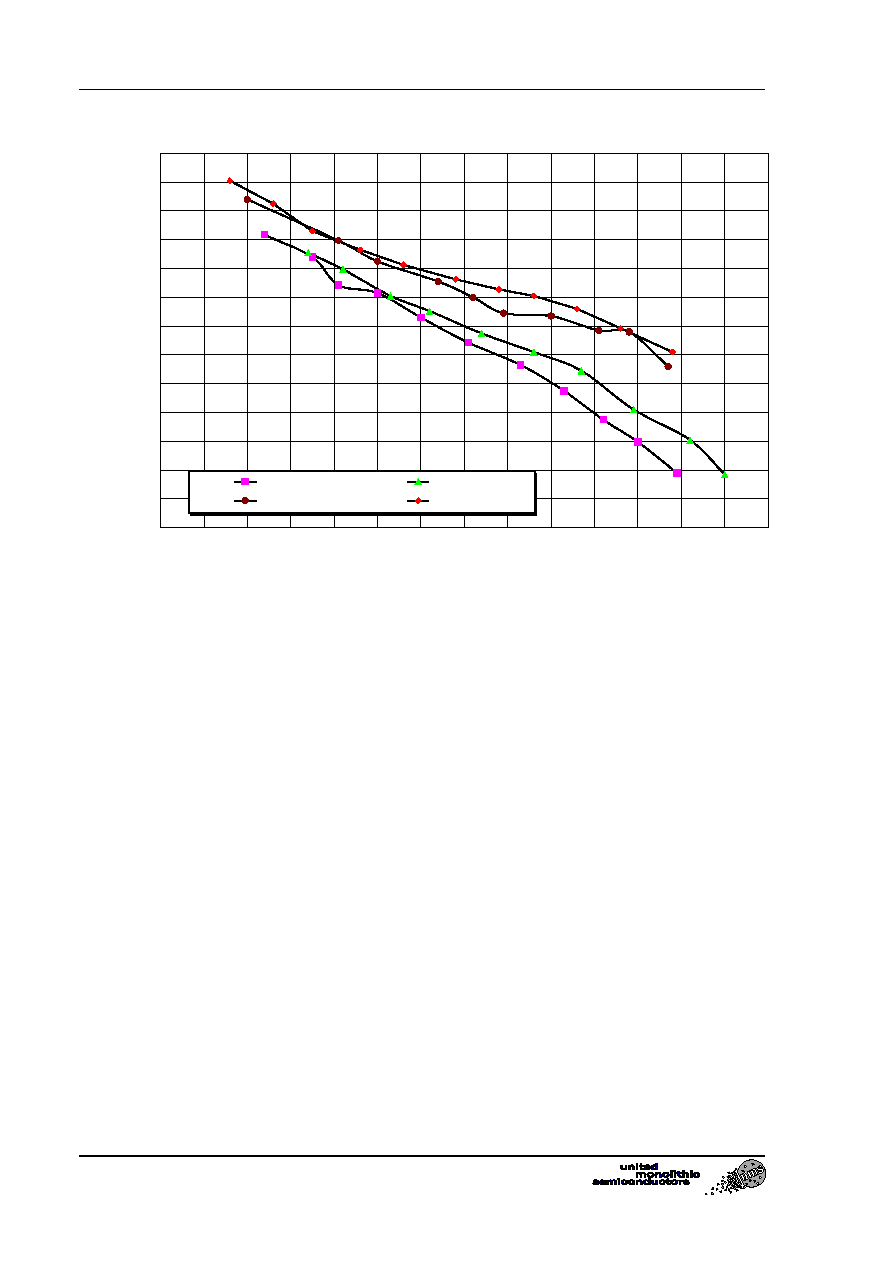
C/I3 versus total output power (
F =10MHz)
26
28
30
32
34
36
38
40
42
44
46
48
50
52
8
9
10
11
12
13
14
15
16
17
18
19
20
21
22
Pout (dBm)
C/I3
(dBc)
17.5GHz
19.5GHz
21.5GHz
23.6GHz
18-24GHz Medium Power Amplifier
CHA5290
Ref. DSCHA52902295 -22-Oct.-02
5/6
Specifications subject to change without notice
Route DÈpartementale 128 , B.P.46 - 91401 ORSAY Cedex - FRANCE
Tel.: +33 (0)1 69 33 03 08 - Fax : +33 (0)1 69 33 03 09
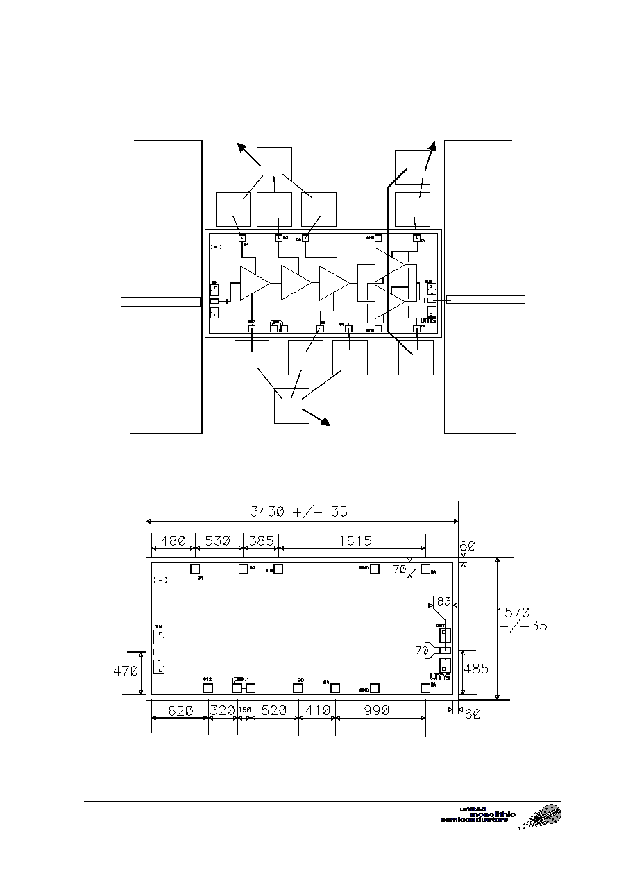
Chip Assembly and Mechanical Data
120pF
120pF
120pF
120pF
120pF
120pF
120pF
120pF
10nF
10nF
10nF
To Vd1,2,3 DC Drain supply feed
To Vd4 DC Drain supply feed
To Vg1,2,3,4 DC Gate supply
Note : Supply feed should be capacitively bypassed. 25µm diameter gold wire is to be prefered.
Bonding pad positions.
( Chip thickness : 50µm. All dimensions are in micrometers )